
The PCB Assembly Process: Most People Miss 70% of It—And It Costs Them Thousands
What is the PCB assembly process? It’s the end-to-end workflow that turns a bare fiberglass PCB and a list of components into a working electronic circuit. Most clients only know the basic “stick parts on board” part. The hidden steps—DFM checks, precise soldering, multi-layer inspection, and post-assembly cleaning—are where 90% of cost overruns and product failures happen.
Why Your "Simple Assembly" Always Turns Into A Disaster
I’ve lost count of how many times an engineer walks in saying “this is a straightforward board, just assemble it.” They see PCBA as a commodity. They shop for the lowest per-unit price and expect perfect results.
It never works that way.
Three months ago, a consumer electronics startup came to us with 2,000 dead boards. They’d used a cheap assembler who skipped every non-mandatory step. The boards had cold joints, tombstoned components, and even leftover flux residue that was corroding the traces. The assembler told them “that’s just how assembly works.”
The real problem? The startup never asked what was included in the quote. They didn’t know that a proper PCB assembly process has 12+ steps, not 3. The cheap shop only did stenciling, pick-and-place, and a quick visual check. Fixing their mess cost them $85,000 and missed their holiday sales window.
If you don’t understand every step of the process, you’re not buying assembly. You’re buying a gamble.
What Actually Happens Step-By-Step (From Someone Who’s On The Floor Weekly)
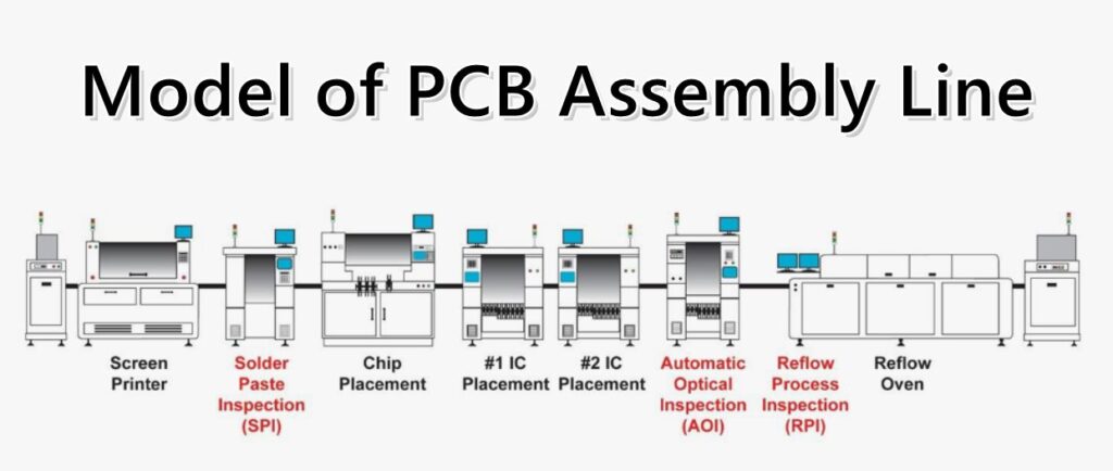
Let’s break this down exactly as it happens in a reputable factory, using the same standards we follow for IPC Class 3 production.
First, we run a full DFM (Design for Manufacturability) check. This happens before any parts are ordered. We look for component spacing issues, incorrect pad sizes, missing thermal reliefs, and obsolete parts. A good DFM check catches 80% of potential failures before they cost you money. If you’re still confused about the basics, start with our guide [What does PCBA mean?]—it will save you from making rookie mistakes.
Next comes solder paste stenciling. We use a laser-cut stainless steel stencil to apply paste made of 96.5% tin, 3% silver, and 0.5% copper. The thickness has to be exact to within 10 microns. Too much paste causes shorts; too little causes weak joints. Cheap shops use worn-out stencils and skip paste inspection—this is the #1 cause of rework.
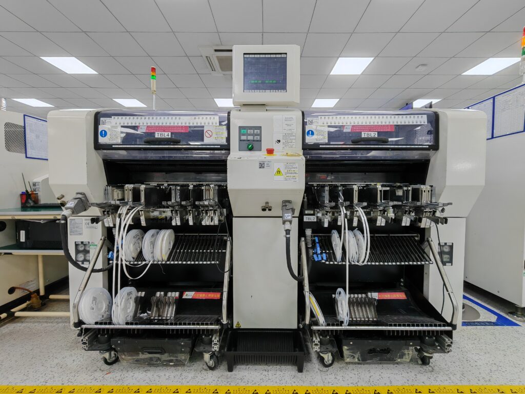
Then the pick-and-place machines go to work. Modern machines place up to 100,000 components per hour, including 01005 packages smaller than a pencil point. They don’t make mistakes—unless your Gerber files or BOM are wrong. We spend more time fixing client BOM errors than we do assembling boards.
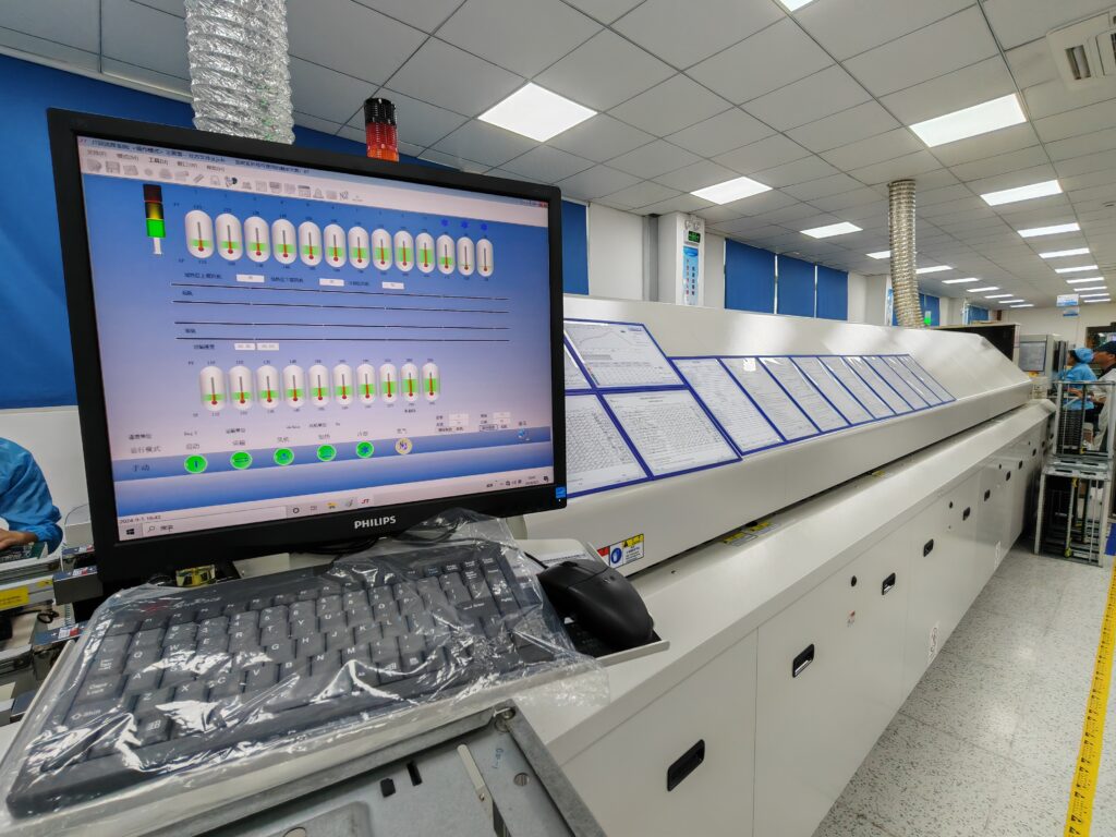
After placement, the board goes through a reflow oven that heats it gradually to 250°C (480°F). The temperature profile is calibrated for every board type. Get it wrong, and you’ll damage sensitive ICs or get cold joints. For double-sided boards, we run this process twice, starting with the side that has smaller components.
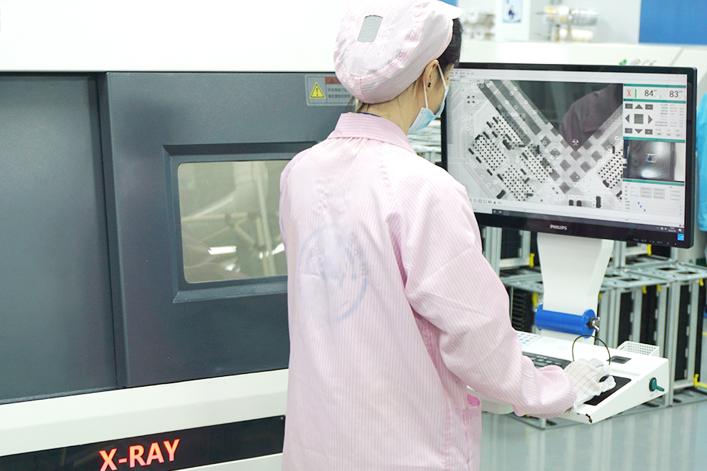
Now comes inspection. We use three methods:
- Manual visual checks for small batches
- AOI (Automatic Optical Inspection) for high-volume runs
- X-ray inspection for BGA and hidden components
Cheap shops skip AOI and X-ray entirely. They’ll ship you boards with hidden shorts that only fail after 6 months of use.
If your board has through-hole components, we use either wave soldering for high volume or hand soldering for small runs. Wave soldering washes the bottom of the board with a wave of molten solder at 500°F. It’s fast, but it can damage delicate components if not done correctly.
Finally, we run a full functional test to make sure the board works as designed. Then we wash it with deionized water to remove flux residue. Flux is acidic—if left on the board, it will corrode the traces over time. Most cheap assemblers skip this step entirely.
SMT vs THT vs Mixed Assembly: Which Is Right For You?
This is the question I get every single day. Here’s the unvarnished comparison based on 10 years of production experience:
| Feature | SMT (Surface Mount) | THT (Through-Hole) | Mixed Assembly |
|---|---|---|---|
| Component Size | 01005 and smaller | Only large components | All sizes |
| Assembly Speed | Extremely fast (fully automated) | Slow (mostly manual) | Medium |
| Cost Per Unit (High Volume) | Lowest | Highest | Medium |
| Mechanical Strength | Low | Highest | Medium |
| Best For | Most modern electronics | Connectors, transformers, power parts | 90% of real-world products |
| Rework Difficulty | High | Low | Medium |
| Lead Time | 2-3 weeks | 3-4 weeks | 3-4 weeks |
The reality is almost no one uses pure THT anymore. 90% of boards we build are mixed technology. The mistake people make is overusing through-hole parts when SMT would work just fine. Every through-hole component adds at least $0.50 to your per-unit cost.
The Truth Your Assembler Will Never Tell You
I spend 3 days a week on production floors. Here’s what no one will say out loud.
Your BOM is probably wrong. Missing part numbers, incorrect footprints, and obsolete components cause 60% of assembly delays. We once had a client send a BOM with a part number that was discontinued in 2019. They didn’t notice until we told them.
Counterfeit parts are everywhere. A $0.05 fake resistor can destroy a $200 board. Reputable assemblers only source from authorized distributors. If a quote seems too good to be true, they’re using gray market parts.
Cleaning isn’t optional. I’ve seen boards fail after 2 years because of unwashed flux residue. The corrosion happens slowly, and by the time you notice, you’re looking at a full product recall.
2026 PCB Assembly Trends: What’s Actually Being Installed Right Now
I don’t do hype. I watch what factories are buying.
By the end of 2026, 70% of mid-to-high volume PCBA shops will have upgraded to AI-powered AOI systems. Traditional AOI misses about 15% of defects. AI-powered systems reduce that to less than 2%. Early adopters are already seeing a 30% drop in rework costs.
We’re also seeing selective soldering replace wave soldering for through-hole components. By 2026, 50% of through-hole assembly will use selective soldering. It’s cleaner, more precise, and causes less damage to SMT components on the same board.
Real Questions, Real Answers
These are the two questions clients ask me most often, but almost no one answers honestly.
Q: Why do quotes for the same board vary by 60% or more?
A: Because they’re not quoting the same service.
A $5 per board quote usually includes: stenciling, pick-and-place, reflow, and a 5-second visual check. It does not include DFM, AOI, X-ray, functional testing, or cleaning. They’ll also hit you with hidden fees for stencils, setup, and rework.
A $8 per board quote from a reputable shop includes all of those things. It also includes the expertise to catch problems before production. The cheapest quote is almost never the cheapest in the end.
Q: Why does my assembler keep asking me to change my design?
A: Because your design is hard to manufacture.
Most engineers design for functionality, not manufacturability. A 0.1mm increase in component spacing can cut your assembly cost by 20% and double your yield. A good assembler isn’t being difficult—they’re saving you money.
If an assembler never asks you to change anything, run. They’re just going to build your bad design and send you the bill for all the scrap.
Ready To Get A Quote That Actually Means Something?
If you’re tired of assemblers who hide fees, miss deadlines, and deliver defective boards, we can help. We’ve been doing this for 10 years, and we follow IPC Class 3, RoHS, and ISO 9001 standards for every project.
Send us your Gerber files and BOM, and we’ll give you a free, no-obligation DFM check and an all-inclusive quote within 24 hours. No hidden fees, no fine print, just honest advice from people who actually build boards every day.
Drop us an email at wm-sales-01@jkr-pcba.com or fill out the form on our website. We’ll get back to you right away.
About US
Founded in 2012, JKRGLO strives to build a one-stop platform for the electronic industry chain. By integrating PCB manufacturing, component procurement and PCB assembly services, we enable digital PCBA processing. With increasing investment in innovation and digital systems, we have achieved rapid growth and emerged as a leading PCB and PCBA manufacturer in the industry, capable of rapidly producing high-reliability and cost-effective products.