
PCB Assembly (PCBA): What It Is, How It’s Built, and How It Differs from a Bare PCB
A bare circuit board, on its own, does nothing. It has copper traces and pads and holes, and no way to think, switch, or regulate anything. PCB assembly is the step that changes that, and it is where most of the money, most of the risk, and almost all of the field failures in an electronics programme actually live.
We build and assemble boards at JKRGLO, so this is the version of the explanation we give on a customer call rather than the version you find in a glossary. What PCB assembly actually is, how a bare board becomes a finished PCBA, which of the eight production steps decide your yield, how assemblies are tested, what drives the quote, and the quality standards a serious supplier should be working to.
If you are only here to settle a naming argument, the next four sentences are the whole answer. Everything after them is the detail.
Quick answer
PCB assembly (PCBA) is the manufacturing step in which electronic components are placed and soldered onto a bare printed circuit board to produce a functional electronic assembly. PCBA stands for Printed Circuit Board Assembly.
A PCB (printed circuit board) is the bare board: the substrate, copper traces, pads, and vias, with no components attached. A PCBA is that same board after components have been mounted and soldered, at which point it can power on and perform its intended function.
PCB fabrication and PCB assembly are two different production stages. Fabrication produces the bare board from Gerber data; assembly buys the components, places them, solders them, and tests the result. Fabrication is a chemistry and imaging process; assembly is a placement, thermal, and supply-chain process.
PCB assembly uses two main technologies. Surface mount technology (SMT) places components directly onto solder-paste-covered pads on the board surface and reflows them in an oven. Through-hole technology (THT) inserts component leads through drilled holes and solders them on the opposite side, usually by wave or selective soldering. Most modern boards use both, which is called mixed-technology assembly.
The single most useful question to ask about any PCBA quote is not the price per board. It is which tests are included. Cheap quotes are almost always cheap because a test stage was quietly removed, and an untested board fails in the customer’s hands rather than on the production line.
What Is PCB Assembly?
PCB assembly is the process of mounting and soldering electronic components onto a fabricated printed circuit board so that the board becomes electrically functional. The result is called a PCBA, short for printed circuit board assembly. Without assembly, a PCB is an inert structure: it can be stored, shipped, and sold, but it cannot perform any electronic function.
The work is easy to describe and hard to do consistently. Components arrive in reels, tubes, and trays. Solder paste is printed onto the pads through a stencil. Placement machines put each component in its exact coordinate and rotation. The board passes through a reflow oven and the paste becomes metal. Then the parts of the job nobody puts on a sales page begin: paste inspection, optical inspection, X-ray of hidden joints, in-circuit test, functional test, cleaning, coating, and traceability.
A typical consumer motherboard carries well over a thousand joints, and modern placement machines handle parts as small as 01005, which is 0.4 mm by 0.2 mm. At that scale there is no useful visual inspection by eye, and no way to rework a joint that has already been covered by a package. Every step either builds quality in or makes it impossible to recover. That is why the process matters more than the equipment list.
The naming problem: five words for two things
Most confusion about PCB assembly is not technical. It is people using four different names for the same object, and one name for something else entirely. Sort the vocabulary first and the rest of the article reads cleanly.
| Term | What it actually means | Where you meet it |
|---|---|---|
| PCB | Printed circuit board. The bare, unpopulated board: substrate, copper traces and planes, pads, vias, solder mask, silkscreen. Non-functional on its own. | Fabrication quotes, board drawings, impedance specs |
| PCBA | Printed circuit board assembly. The board after components are mounted and soldered. Electrically functional and ready to integrate. | Assembly quotes, BOM reviews, test reports |
| PCB assembly (the process) | The set of operations that turn a PCB into a PCBA: paste printing, placement, reflow, through-hole soldering, inspection, test. | Process documents, DfM reports, factory audit checklists |
| PCB fabrication | The separate upstream process that builds the bare board: imaging, etching, lamination, drilling, plating, surface finish. | Fabrication orders, stack-up discussions |
| EMS / contract manufacturer | Electronics manufacturing services. A company that performs assembly, and often fabrication, sourcing, coating, box build, and logistics as one contract. | Supplier selection, NDA and quality agreements |
| Box build | The stage after PCBA where the tested assembly is fitted into its enclosure with wiring, displays, and hardware. | Turnkey programmes, finished-goods shipments |
PCB assembly is a manufacturing process; a PCBA is the product of that process. Saying “I need PCB assembly” means you need the work done. Saying “I need 500 PCBAs” means you need 500 finished, populated, tested boards delivered.
One more distinction saves a lot of quoting friction. Fab houses and assembly houses are not always the same company, and the two quotes you receive are for different scopes. If you ask three suppliers for “a PCB quote” and only one of them prices the components, you are not comparing three prices for one thing. You are comparing three different scopes. The scope that matters is the one that ends in a tested PCBA, because that is the only deliverable that can be powered up.
If you are still sorting out the board itself, the components that go on it are covered in circuit board parts and components, and the board-level upstream process is covered in PCB fabrication services.
PCB vs PCBA: The Difference That Changes Your Quote
The difference between a PCB and a PCBA is components. A PCB is the bare board with no parts attached and no electronic function. A PCBA is the same board after components have been placed and soldered, and it performs the function the circuit was designed for. Everything else — cost structure, lead time, defect types, and test requirements — follows from that one difference.
This distinction is not academic. The two stages are quoted separately, produced by different equipment, measured against different standards, and fail in completely different ways. A bare board that passes electrical test can still become a PCBA that fails in the field, and the reason will have nothing to do with the board.

| Aspect | PCB (bare board) | PCBA (assembled board) |
|---|---|---|
| What it is | Substrate with copper traces, pads, and vias; no components | The same board populated with components and soldered |
| Function | Provides the physical and electrical platform for components | Performs the actual electronic function |
| Production process | Imaging, etching, lamination, drilling, plating, surface finish | Solder paste printing, placement, reflow, through-hole soldering, inspection, test |
| Cost structure | Driven by layer count, board size, material, copper weight, surface finish | Driven by component cost, BOM line count, placement count, and testing scope |
| Where the money is | Tooling and material, largely predictable | Components and process control, highly variable between suppliers |
| Typical defect types | Trace shorts and opens, drill misalignment, delamination, poor surface finish | Insufficient or excess solder, tombstoning, bridging, polarity errors, voids under BGA |
| Standard test | Electrical test on the bare board: flying probe or dedicated fixture | SPI, AOI, X-ray, in-circuit test, functional test, sometimes burn-in |
| Lead time profile | Short: days for standard boards | Longer and less predictable: gated by component availability |
| Who owns it | Often a fabrication house | Often an assembly house or an EMS provider |
| Failure mode that hurts most | A short or open that ships inside the board | A joint that looks perfect and fails after thermal cycling |
Why the difference decides whether your quote is comparable
When two PCBA quotes for the same design differ by 30%, the difference is almost never in the placement labour. It is in the three things that are invisible on a quotation PDF:
- Component sourcing channel. Authorised-distributor parts and open-market “surplus” parts can look identical in a BOM line and behave completely differently in the field. Ask which distributors are used, and ask what incoming inspection is applied to parts that do not come from a franchised source.
- Test coverage. AOI on every board, or AOI on the first article only? X-ray on every BGA, or only when a customer complains? 100% functional test, or a sample? The test plan is where the cost difference actually sits.
- Process discipline on the invisible steps. Stencil cleaning frequency, paste age and storage, reflow profile verification, moisture-sensitive part baking, ESD controls. None of it appears on an invoice. All of it appears in your field failure rate.
The most expensive PCBA you will ever buy is the cheap one that fails after it ships. A lower unit price that includes less testing does not reduce your cost; it moves the cost from your supplier’s factory to your customer’s hands, and adds shipping, replacement labour, and reputation damage on the way.
If you only take one operational habit from this article, take this one: request the test plan in writing as part of the quote, in the same way you would request the BOM. A supplier who can describe their test coverage in specific terms is a supplier who runs one. The broader sourcing comparison is covered in how to choose a PCBA manufacturer.
The PCB Assembly Process, Step by Step
The PCB assembly process runs in eight stages: design and DfM review, documentation and stencil preparation, solder paste printing, component placement, reflow soldering, through-hole and mixed-technology soldering, inspection, and electrical and functional testing. Each stage has a defect it is responsible for, and most assembly failures can be traced back to a specific stage rather than to vague “poor quality”.
This is the sequence an assembly line follows for a surface-mount board. Through-hole-only and mixed boards insert extra steps in the middle, which are covered in the next section.
| # | Stage | Equipment | The defect this stage creates |
|---|---|---|---|
| 1 | Design and DfM review | Engineering review of Gerbers, BOM, and CPL | Wrong footprints, unmanufacturable clearances, single-sourced or obsolete parts, untestable nets |
| 2 | Documentation and stencil | Laser-cut stainless steel stencil, aperture engineering | Wrong paste volume from a bad aperture ratio, leading to opens or bridges later |
| 3 | Solder paste printing | Solder paste printer, squeegee, SPI station | Insufficient, excessive, or misaligned paste; the root cause of most reflow defects |
| 4 | Component placement | Pick-and-place machine, feeders, vision alignment | Misplacement, rotation errors, wrong part, reversed polarity, damaged fine-pitch leads |
| 5 | Reflow soldering | Multi-zone convection reflow oven | Cold joints, tombstoning, voids, package cracking, warpage if the profile is wrong |
| 6 | Through-hole and mixed soldering | Wave, selective, or hand soldering with IPC-certified operators | Incomplete barrel fill, solder bridges between adjacent pins, thermal damage to nearby parts |
| 7 | Inspection | SPI, AOI, X-ray (AXI), visual inspection under magnification | Defects that are present but not detected, and reach the customer |
| 8 | Electrical and functional test | ICT fixture or flying probe, FCT rig, burn-in chamber | Marginal units that pass inspection and fail in application |
Step 1 – Design and DfM review
Nothing is built yet and this is where the most money is saved or lost. A design-for-manufacturing review asks whether the board can actually be built at the quoted yield: are pads large enough for the component and the process, is there enough clearance for the placement nozzle and the reflow airflow, are any parts single-sourced with a 40-week lead time, and can every critical net actually be probed by a test fixture?
A pad designed 0.1 mm too small costs nothing to change on a Friday afternoon and costs a stencil revision, a re-spin, and two weeks if it is found after tooling. This is also the stage where design-for-assembly and testability considerations get folded in, because a net that cannot be probed cannot be tested, and an untestable board is an unverifiable one.
Step 2 – Documentation and stencil preparation
Assembly needs four data sets before anything moves: Gerber or ODB++ fabrication data, a BOM with manufacturer part numbers and quantities, a pick-and-place file (also called a centroid or CPL file) giving X–Y coordinates and rotation for every component, and an NC drill file. An assembly drawing carries the requirements that do not fit in the machine data, such as connector orientations, stiffener placement, and coating zones.
The stencil is laser-cut stainless steel with apertures matched to the pad pattern. Stencil thickness sets the paste volume, and typical production stencils run about 0.10 mm to 0.15 mm. Getting the area ratio right for fine-pitch parts is an engineering task, not a purchasing one.
Step 3 – Solder paste printing
The stencil is aligned over the board and solder paste is spread across it with a squeegee, so that paste is deposited only on the pads. Solder paste is not solder; it is a suspension of fine solder powder in flux, and both halves matter. The flux cleans the surfaces and controls oxidation during reflow, and the powder determines the alloy and the melting behaviour.
Most reflow defects originate here rather than in the oven. Too little paste produces an open or a weak joint. Too much produces bridging and, on fine-pitch parts, tombstoning. Solder paste inspection (SPI) exists precisely to catch this before components are placed, because a paste defect is cheap to fix at this point and impossible to fix afterwards.

Step 4 – Component placement
Pick-and-place machines read the CPL file, pick components from reels and trays with vacuum nozzles, verify orientation and package geometry with vision systems, and place each part onto its paste-covered pads. Modern machines place tens of thousands of components per hour and hold placement accuracy in the tens of microns, which is what makes 0201 and 01005 parts practical at all.
Feeder setup is the quiet failure point. A reel loaded with a visually similar but electrically different part, or a feeder that misfeeds intermittently, produces boards that pass inspection and fail in the field. This is why incoming inspection and BOM-to-reel verification are not administrative overhead.

Step 5 – Reflow soldering
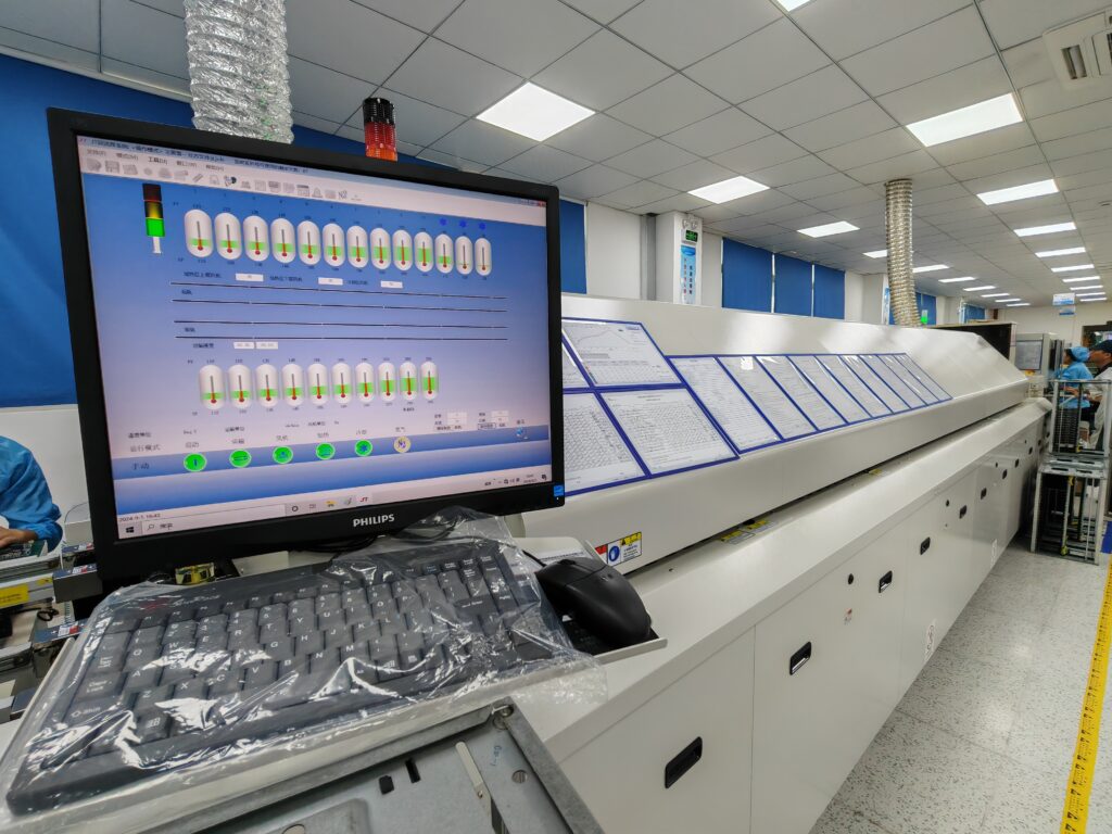
The populated board travels through a multi-zone convection oven on a conveyor. The thermal profile has four phases: preheat, where the board and components come up to temperature gradually; soak, where the flux activates and the assembly equalises; reflow, where the alloy melts and wets the pads and leads; and cooling, where the joint solidifies.
The numbers are set by the alloy and the components, not by preference. Lead-free SAC305 (tin–silver–copper) melts around 217 °C to 220 °C and is normally run with a peak of roughly 235 °C to 250 °C, while eutectic tin–lead Sn63Pb37 melts at 183 °C. Every component on the board also has a maximum temperature and a maximum ramp rate it will tolerate, and the profile has to satisfy all of them at once. A profile that is 10 °C too hot degrades parts silently; one that is too cold leaves joints that look acceptable and crack under thermal cycling.
Nitrogen is sometimes used in the oven to reduce oxidation and improve wetting on fine-pitch and high-reliability work. Moisture-sensitive components must be baked or dry-stored before reflow, otherwise absorbed moisture flashes to steam inside the package during the ramp and cracks it from the inside.
Step 6 – Through-hole and mixed-technology soldering
Not everything can be surface mounted. Connectors, large electrolytics, transformers, terminal blocks, and parts that must survive mechanical load are through-hole, because a lead that passes through the board and is soldered on the far side holds far better under insertion and vibration forces than a surface pad does.
- Wave soldering passes the underside of the board over a standing wave of molten solder, soldering every exposed through-hole lead in one pass. It is fast and suited to volume.
- Selective soldering applies solder to individual joints with a small nozzle. It is slower but avoids heating the whole board, which matters when there are temperature-sensitive parts already reflowed on the top side.
- Hand soldering is used for repairs, prototypes, and odd-form parts that no machine can place. It is the most operator-dependent method, which is why workmanship standards and operator certification matter more here than anywhere else on the line.
Step 7 – Inspection
Inspection is a set of overlapping filters rather than a single checkpoint, and each filter sees something the others cannot. SPI sees the paste. AOI sees visible joints and placement. X-ray sees joints hidden under a package. Visual inspection under magnification sees the things no algorithm was trained on. The specifics are compared in the testing section below, and the inspection philosophy behind them is covered in AOI inspection and quality control in PCB manufacturing.
Step 8 – Electrical and functional test
In-circuit test (ICT) uses a bed-of-nails fixture or a flying probe to verify continuity, component values, and the absence of shorts and opens, net by net. Functional test (FCT) powers the assembly up in a rig that simulates the real application, applying power, stimulus, and loads, and checks that the product does what the specification says. For complex boards, FCT is the last real quality gate before shipping, and for safety-critical products it is followed by burn-in.
These stages are covered in more depth in the full assembly process guide, and the test strategy itself in how PCBA testing works.
SMT, Through-Hole, and Mixed Assembly: Which One You Actually Need
Surface mount technology (SMT) places components directly onto solder-paste-covered pads on the board surface and solders them by reflow, while through-hole technology (THT) inserts component leads through drilled holes and solders them on the opposite side. Mixed-technology assembly uses both on the same board, which is the normal case for most industrial and consumer products.
The choice is not a preference between old and new. Each technology solves a different problem, and most boards need both because they need both a dense logic section and mechanically robust connections.
| Dimension | SMT | Through-hole (THT) | Mixed |
|---|---|---|---|
| How it attaches | Component sits on pads on the board surface | Leads pass through drilled holes and are soldered on the far side | SMT first, then THT inserted and soldered |
| Board area used | Low: parts sit flat, both sides usable | High: needs a hole and a pad footprint per lead | Between the two |
| Mechanical strength | Moderate; joints resist shear poorly | High; the hole and barrel carry insertion and vibration load | High where it is needed |
| Typical parts | Resistors, capacitors, ICs, QFN, BGA, CSP, LEDs | Connectors, large electrolytics, transformers, terminal blocks, power devices | Real-world boards with a logic section and an interface section |
| Soldering method | Reflow in a multi-zone oven | Wave, selective, or hand soldering | Reflow, then wave or selective |
| Placement speed | Very fast, fully automated | Slower; insertion is partly manual | Slower overall |
| Cost at volume | Lowest per joint | Highest per joint | Adds a second process stage |
| Main limitation | Poor mechanical robustness under load | Consumes board area and adds drilling | More process steps, more controls to verify |
How to decide
- If the part is available in a surface-mount package and does not carry mechanical or high-current load, use SMT. It is cheaper, denser, and better at high frequency.
- If the part must survive cable insertion force, vibration, or thermal cycling of a heavy body, use through-hole. A connector that is only surface mounted will eventually lift its pads under repeated cable stress.
- If the part is a high-power device that needs to dump heat into the board, through-hole or a thermal pad with vias is usually required, because the copper mass and the hole give a much better thermal path.
- If a design is all-SMT because it was cheaper on paper, the field failures will cluster at the connectors and the power section, which is exactly where designers did not want them.
A practical note on mixed boards: through-hole parts soldered by wave or selective soldering are exposed to a second thermal cycle after the SMT reflow. Components already on the top side must tolerate it, and this is one of the constraints a DfM review is checking for. If you are choosing packages for a new design, the three main types of PCBs and PCB material selection cover the board-level decisions that sit underneath this one.
There is also a flexible variant of this decision. When the board itself has to bend, SMT is still used but the assembly rules change, because components and stiffeners must be kept out of bend zones. That is the subject of flexible circuits.
How a PCBA Is Tested, and What Each Test Actually Catches
PCBA testing uses complementary methods rather than one definitive test: solder paste inspection (SPI) verifies paste deposition before placement, automated optical inspection (AOI) verifies visible joints and component placement after reflow, X-ray or AXI inspects joints hidden beneath packages such as BGA and QFN, in-circuit test (ICT) verifies electrical continuity and component values, and functional test (FCT) verifies that the assembly works in its intended application.
The reason there are so many methods is that no single one can see everything. A cold joint under a BGA is invisible to AOI. A reversed but correctly soldered component is invisible to X-ray. A component with the right value but a marginal tolerance passes ICT and fails FCT. Testing is designed as a layered defence, and the layers are chosen from the failure modes the design is actually exposed to.
| Method | When it runs | What it sees | What it cannot see |
|---|---|---|---|
| SPI (solder paste inspection) | After printing, before placement | Paste volume, area, height, and alignment on every pad | Anything that happens after placement |
| AOI (automated optical inspection) | After reflow, and often after placement too | Missing, misplaced, or rotated parts; polarity; bridges; visible solder fillets; some text and package damage | Joints hidden under BGA, QFN, and LGA packages; electrical behaviour |
| X-ray / AXI (automated X-ray inspection) | After reflow | Hidden joints, voids, insufficient solder, head-in-pillow and open joints under area-array packages | Component values; anything not related to solder geometry |
| Flying probe | After assembly, on prototypes and low volume | Continuity, shorts, opens, and component presence without a dedicated fixture | Speed, and behaviour at power; fixture-based node access |
| ICT (in-circuit test) | After assembly, in volume | Net-by-net continuity, short and open detection, component value verification | Whether the product functions in its real application |
| FCT (functional test) | Final stage before shipping | Real operating behaviour with power, stimulus, and loads applied | Defects that only appear under environmental stress |
| Burn-in / environmental | Where reliability is critical | Early-life failures under temperature cycling, humidity, or continuous power | Design margin; defects that need longer than the burn-in window to appear |
| Visual inspection | Throughout | Odd-form conditions, coating coverage, mechanical damage, workmanship | Anything at a scale below the magnification used |

In-circuit test verifies that the board is built correctly; functional test verifies that the board works. A PCBA can pass ICT and fail FCT, because a board can be electrically correct and still behave incorrectly when it is powered up in its real application. High-reliability programmes require both.

Why test coverage is the real content of a quote
Test coverage is the honest measure of how much a supplier is willing to guarantee. It is also the first thing removed when a price has to come down, because it is invisible: nobody can see the test that was not run, and the boards still ship on time.
A PCBA that is not functionally tested has not been verified, only assembled. If the quote does not state which tests are included, at what coverage, on what proportion of boards, then the price is not comparable with one that does.
Workmanship for all of these inspections is judged against the IPC-A-610 standard, which defines what an acceptable joint, placement, and fillet look like, and what must be rejected. The wider reliability programme around it is covered in quality control in PCB manufacturing.
What Actually Drives PCB Assembly Cost
PCB assembly cost is driven by component cost, the number of BOM line items and placement positions, board complexity and layer count, the test scope, the quantity, and any added processes such as conformal coating or box build. Component cost, not placement labour, is usually the largest single line in a modern PCBA quote.
This is the part of the conversation where expectations usually diverge. Buyers assume the labour of placing parts dominates the price. In practice, on a modern board, the components dominate, and the assembly labour is a smaller share than almost anyone expects until they see their first quote with the BOM priced separately.
| Cost driver | Why it moves | How to influence it |
|---|---|---|
| Components | Usually the largest line item; dominated by ICs, and moved by allocation, lifecycle status, and MOQ | Standardise part numbers, prefer multi-sourced passives, avoid single-source long-lead parts |
| Number of BOM lines and placements | Every unique part adds feeder setup, verification, and rework risk | Reduce unique part numbers; use resistor and capacitor arrays where sensible |
| Board complexity | Layer count, fine-pitch parts, and via-in-pad all raise process difficulty | Keep the stack-up no more complex than the design needs |
| Test scope | ICT fixtures, X-ray coverage, and FCT rigs carry real cost | Choose tests by failure mode, not by default; reuse fixtures across revisions |
| Quantity | Setup and tooling amortise; volume reduces per-unit cost | Consolidate orders; avoid quantities that sit between price bands |
| One-time charges (NRE) | Stencils, programming, fixtures, and first-article inspection are charged once | See below: NRE is a one-off, not a per-board cost |
| Added processes | Conformal coating, underfill, depanelisation, and box build are separate operations | Specify only what the operating environment requires |
| Lead time and expediting | Sourcing from the spot market and running partial shifts costs more | Share a realistic schedule early; avoid emergency sourcing |
Where cheap and expensive quotes actually differ
Two quotes for an identical BOM and Gerber set can differ substantially without either supplier lying. The difference sits in four places: the sourcing channel for components, the amount of incoming inspection on those components, the test coverage on finished boards, and the amount of process control applied to paste, profile, and moisture-sensitive parts.
A supplier who sources from franchised distributors and inspects what arrives pays more for parts and less for scrap. A supplier who buys from the open market pays less for parts and carries counterfeit and refurbished-part risk that lands in your field returns. Both can print a competitive number. Only one of them will still be credible in eighteen months.
One-time charges deserve separate treatment, because buyers routinely compare them against the wrong baseline. NRE covers stencils, machine programming, fixture fabrication, and first-article inspection. It is paid once, not per board, so it dilutes with volume and should never be compared across different quantities. The composition and negotiation of these charges is covered in NRE and one-time engineering charges, and unit-cost structure in what drives PCB assembly cost.
What to Send for a PCB Assembly Quote
A PCB assembly quote requires four data sets: Gerber or ODB++ fabrication data, a bill of materials (BOM) listing every component with a manufacturer part number and quantity, a pick-and-place or CPL file giving the X–Y coordinate and rotation of every component, and an NC drill file. An assembly drawing, a test specification, and the required quantity and target schedule complete the package.
Missing documentation is the most common reason a quote takes a week instead of a day, and the second most common reason a production build stops halfway. The list below is short, and every item on it exists because its absence causes a specific failure.
| Document | What it contains | What breaks without it |
|---|---|---|
| Gerber / ODB++ | Copper layers, solder mask, silkscreen, outline, and drill data for fabrication | Nothing can be built; the board data itself is missing |
| Bill of materials (BOM) | Every component with reference designator, description, manufacturer part number, and quantity per board | Components cannot be sourced or verified; substitutions get made without your approval |
| Pick-and-place / CPL file | X–Y coordinates and rotation for every component placement | Placement must be reverse-engineered from the Gerbers, which introduces rotation errors |
| NC drill file | Hole positions and diameters | Drilling and via formation cannot be verified against the design intent |
| Assembly drawing | Connector orientations, stiffener or shield placement, coating zones, torque and mechanical notes | Ambiguity is resolved by the supplier rather than by you |
| Test specification | Required test coverage, test points, pass criteria, and any functional rig requirements | The cheapest available test scope is assumed rather than the one you need |
| Quantity and schedule | Order quantity, build phases, and required delivery dates | Costing is done at the wrong volume; lead-time risk is not surfaced early |
| Approved-vendor and quality notes | Required certifications, IPC-A-610 class, and any approved-substitute rules | A board is built to a standard you did not specify |
The BOM is where most quotes go wrong
A BOM is not a shopping list, it is a contract. If a line says only “10 µF capacitor” with no manufacturer part number, the supplier must choose, and their choice will be driven by cost and availability rather than by your electrical and thermal requirements. Both are defensible positions; only one of them is your design.
List manufacturer part numbers, and state which substitutions are acceptable. Mark critical parts as no-substitute. Note lifecycle status for anything you intend to build for more than two years, because a part in its last-time-buy window will need a documented second source eventually, and finding out during a shortage is the expensive way to learn it.
If your BOM has line items with no manufacturer part number, you have not defined your product — you have described a category. Fill those in before you send the file, or accept that the component choice has been delegated.
Once the package is complete, send us your Gerbers and BOM for a DFM review. A design review before production costs nothing and routinely catches the issues that would otherwise appear as yield loss.
Which Quality Standard Should Your PCBA Be Built To?
IPC-A-610 is the industry standard for the acceptability of electronic assemblies, defining what an acceptable solder joint, component placement, and assembly condition looks like, and what must be rejected. It is applied in three classes: Class 1 for general electronics, Class 2 for dedicated service electronics, and Class 3 for high-performance and life-critical products.
Class is the single most useful field on a purchase order that buyers routinely leave blank, and it is the field that decides what the factory is allowed to accept. A joint that is acceptable at Class 1 is a defect at Class 3, and the same board can legitimately be rejected or shipped depending on which class was specified.
| Class | Intended use | Typical products | What it means in practice |
|---|---|---|---|
| Class 1 | General electronic products where the main requirement is that the assembly functions | Consumer toys, simple accessories, non-critical indicators | Cosmetic and some fillet imperfections are acceptable; the focus is function |
| Class 2 | Dedicated service electronic products with a requirement for continued performance and extended life | Industrial controls, consumer electronics, computers, communications equipment | Tighter fillet and placement criteria; the default expectation for most commercial work |
| Class 3 | High-performance electronic products where continued performance or on-demand reliability is critical | Aerospace, defence, medical devices, life support, safety systems | Highest criteria: full barrel fill, tight void limits, strict rework controls, documented evidence |
Class 2 is the sensible default for most commercial hardware, and Class 3 is a specification you buy deliberately for a reason, not a badge to add for reassurance. Choosing Class 3 on a consumer accessory raises cost and rework rates without changing how the product performs.
The other standards that appear on a serious quality pack
- J-STD-001 covers the materials and process requirements for soldered electrical and electronic assemblies, which is the process-side companion to IPC-A-610’s workmanship criteria.
- IPC-7711 / IPC-7721 covers rework, repair, and modification of assemblies, which matters because unqualified rework is one of the most common ways a good board is turned into a marginal one.
- IPC/JEDEC J-STD-033 covers the handling, packing, shipping, and baking of moisture-sensitive devices, which is the standard that prevents popcorn cracking during reflow.
- ANSI/ESD S20.20 defines the electrostatic discharge control programme, which is the difference between a factory that protects sensitive parts and one that degrades them invisibly.
- ISO 9001 is the baseline quality management system. ISO 13485 applies to medical devices, IATF 16949 to automotive, and AS9100 to aerospace.
Certifications describe which industries a supplier is structurally prepared to serve, not which slogans look good on a homepage. Match them to your product’s regulatory environment and ask to see the certificate and its scope. our certifications and capability window are published for exactly this reason.
A related question is who performs the work. Fabrication, assembly, and box build can sit with one supplier or be split across three, and the split is what determines who is accountable when something fails. The model, its trade-offs, and what the EMS model actually commits a supplier to are worth understanding before you sign a quality agreement.
Common PCB Assembly Defects and What Causes Them
The most common PCB assembly defects are insufficient or excessive solder, solder bridging, tombstoning, component misplacement and rotation errors, reversed polarity, voids and opens under area-array packages, and incomplete through-hole barrel fill. Almost all of them originate in paste printing, placement accuracy, or the reflow profile rather than in the components.
Knowing the defect list is useful mainly because each defect points at a process stage, and a stage can be controlled. “Quality problems” cannot be controlled. A tombstoned capacitor can.
| Defect | What it looks like | Root cause | How it is prevented |
|---|---|---|---|
| Insufficient solder | Weak or concave fillet, intermittent opens | Low paste volume, poor stencil release, pad contamination | Stencil aperture design, SPI feedback loop, paste and board cleanliness |
| Excess solder / bridging | Solder joining two adjacent pads or pins | Too much paste, poor gasketing, wrong squeegee pressure | Stencil and print parameter control, AOI feedback at the printer |
| Tombstoning | Chip component standing on one end | Uneven paste deposits or uneven heating across the two pads | Symmetric aperture design, balanced thermal footprint, profile tuning |
| Misplacement / rotation | Component offset or rotated from its intended orientation | Wrong CPL data, feeder error, vision alignment failure | First-article verification for critical packages, feeder and program checks |
| Reversed polarity | Polarised part installed backwards | Silkscreen ambiguity, wrong reel, no first-article check | Clear polarity marking, reel verification, mandatory first-article inspection |
| Voids and opens under BGA/QFN | Hidden joint defects invisible from outside | Poor wetting, insufficient paste, entrapped flux volatiles, warpage | X-ray inspection, profile optimisation, moisture baking before reflow |
| Incomplete barrel fill | Through-hole joint not filled through the hole | Insufficient flux, wrong wave parameters, thermal mass | Wave or selective soldering parameter control, IPC-A-610 class-driven acceptance |
| Cold joint | Dull, grainy, or irregular solder surface | Peak temperature too low, insufficient time above liquidus, contaminated surfaces | Verified reflow profile, alloy-specific thermal window, cleanliness controls |
| Delamination / warpage | Board distortion after thermal cycling | Excess moisture in the laminate, thermal mismatch, poor handling | Material selection, bake cycles, storage and handling controls |
| Contamination / residue | Flux residue or particulates on the assembly | Incomplete cleaning or skipped wash stage | Specified cleaning process, residue limits, cleanliness verification |

The pattern worth remembering
Read the root-cause column top to bottom and one theme repeats: paste, placement, and profile. Those three stages produce the majority of assembly defects, and all three are process-controlled rather than part-controlled. That is why the meaningful difference between suppliers shows up in their process discipline, not in their component list, and why a supplier who cannot describe their print and profile controls cannot describe their yield either.
There is a commercial consequence too. Defects found at inspection cost the supplier money. Defects that escape inspection cost you money, in replacements, freight, engineering time, and reputation. The test plan in how PCBA testing works is the mechanism that decides which side of the line a defect lands on.
Turnkey, Consigned, or Partial Assembly: Who Owns the Supply Chain
In turnkey PCB assembly the supplier handles bare board fabrication, component sourcing, assembly, and testing under a single contract, and the customer supplies only design files. In consigned assembly the customer supplies some or all components, and the supplier performs only the assembly work. Partial or hybrid assembly splits the two.
This is a commercial decision with a technical consequence. The question is not who is cheapest per board; it is who is accountable when a board fails, and how many parties have to be reconciled before that question can be answered.
| Model | Who supplies what | Who owns the risk | Best for | The catch |
|---|---|---|---|---|
| Turnkey | Supplier builds the board, buys the components, assembles, tests, and ships | Supplier, end to end | Most programmes, especially first builds and volume | You rely on the supplier’s sourcing integrity; verify the authorised-distributor route |
| Consigned | Customer supplies components; supplier assembles | Split: customer owns parts, supplier owns process | Companies with existing inventory, or with parts they must control | Component damage in assembly becomes a dispute; hidden-cost coordination |
| Partial / hybrid | Mix of the two, for example customer supplies critical ICs only | Split at the boundary of each part | Programmes working around allocation on specific parts | Two accountability boundaries to manage instead of one |
| Box build | Everything above, plus integration into the enclosure | Supplier | Products shipping as finished goods | Adds mechanical, cable, and packaging scope to the quality agreement |
Why turnkey usually wins on total cost, even when it loses on unit price
Splitting the chain across vendors looks cheaper on paper because each line item can be bid separately. In practice it creates handoff points, and defects hide in handoffs. When the assembler did not buy the components, every field failure starts the same way: the assembler blames the parts, the parts supplier blames the process, and the schedule absorbs the argument while your launch date moves.
A turnkey supplier owns that entire interface. One team reviews the BOM, builds the board, tests it, and ships it, which means traceability runs from component lot number to serialised assembly, and there is one quality system governing the whole chain. That is worth more than the last few percent of unit price, and it is the reason turnkey PCB assembly is the default model for hardware teams that want to spend their engineers’ time on the product rather than on supplier reconciliation.
The counter-case is real and worth stating plainly: if you already hold inventory, or you must control a specific part for security or performance reasons, consignment can be the right answer. Just make the boundary explicit in writing, including who bears the cost when a customer-supplied part is damaged during assembly.
PCB Assembly: Frequently Asked Questions
1. What does PCBA stand for?
PCBA stands for printed circuit board assembly. It refers both to the process of mounting and soldering components onto a bare PCB, and to the finished populated board that results from that process.
2. What is the difference between a PCB and a PCBA?
A PCB is the bare board: substrate, copper traces, pads, and vias, with no components and no electronic function. A PCBA is that board after components have been mounted and soldered, so that it can power on and perform its intended function. The difference is the components and the assembly work that attaches them.
3. Is PCB assembly the same as PCB fabrication?
No. Fabrication produces the bare board through imaging, etching, lamination, drilling, plating, and surface finishing. Assembly takes that finished bare board, sources the components, places and solders them, and tests the result. They are separate production stages, are often performed by different companies, and are quoted separately.
4. What files do I need for a PCB assembly quote?
Gerber or ODB++ fabrication data, a BOM with manufacturer part numbers and quantities, a pick-and-place (CPL) file with X–Y coordinates and rotations, and an NC drill file. Add an assembly drawing, a test specification, and the required quantity and schedule for a quote that reflects what you actually need rather than the cheapest interpretation of it.
5. What is the PCB assembly process?
The standard sequence is design and DfM review, documentation and stencil preparation, solder paste printing, component placement, reflow soldering, through-hole or mixed-technology soldering, inspection, and electrical and functional testing. Boards that need protection or integration continue into cleaning, conformal coating, and box build.
6. What is the difference between SMT and through-hole assembly?
SMT places components directly onto solder-paste-covered pads on the board surface and solders them by reflow, which allows high density and fast automated production. Through-hole assembly inserts component leads through drilled holes and solders them on the opposite side, usually by wave or selective soldering, which gives far better mechanical strength. Most boards use both.
7. How is a PCBA tested?
Testing is layered. Solder paste inspection verifies paste before placement, automated optical inspection verifies visible placement and joints after reflow, X-ray inspects joints hidden under BGA and QFN packages, in-circuit test verifies electrical continuity and component values, and functional test verifies that the assembly works in its real application. High-reliability products add burn-in or environmental testing.
8. What is turnkey PCB assembly?
Turnkey PCB assembly means one supplier takes responsibility for the entire chain: bare board fabrication, component sourcing, assembly, testing, and often coating and box build. The customer supplies only design files and receives a tested assembly. It removes the coordination and accountability gaps that appear when the chain is split across several vendors.
9. Why do two PCBA quotes for the same design differ so much?
Usually because of three things that are not visible on the quotation itself: the component sourcing channel, the amount of incoming inspection applied to those components, and the test coverage on finished boards. A cheaper quote frequently reflects a reduced test scope rather than a more efficient factory.
10. What is IPC-A-610 and which class do I need?
IPC-A-610 is the industry standard defining acceptable workmanship for electronic assemblies. Class 1 covers general electronics, Class 2 covers dedicated service products and is the sensible default for most commercial hardware, and Class 3 covers high-performance and life-critical products such as aerospace, defence, and medical devices. Specify the class on the purchase order, because it decides what the factory is permitted to accept.
Still working through the board-level picture? circuit board parts and components covers what is on the board, and how PCBA testing works covers how to verify it once it is built.
Get a DFM Review Before You Commit to a Build
The expensive assembly problems are all decided before the first board is built: a BOM line with no manufacturer part number, a pad too small for the process window, a single-sourced part in its last-time-buy window, a connector that is surface mounted where it needs a through-hole anchor, and a test plan that was never written down.
Every one of those is cheap to fix at quotation stage and expensive to fix after a production run has shipped. That is the whole reason we review designs before we quote them, not after.
JKRGLO builds PCB and PCBA under one roof, combining bare board fabrication, component sourcing, SMT and through-hole assembly, testing, and final integration. Send us the Gerbers, the BOM, and the CPL file, and our engineering team will run a DfM and testability review alongside your quotation. If something in the design is going to cost you yield, we would rather say so before you commit to tooling.
send us your Gerbers and BOM for a DFM review · turnkey PCB assembly · our certifications and capability window
JKRGLO is a one-stop PCB and PCBA manufacturer, combining PCB fabrication, component sourcing, assembly, and testing under one roof.
You may also be interested in…

About the Author
Andrew Zhan – R&D Engineer at JKRGLO.com
With over 14 years of R&D engineering experience in the PCB industry, Andrew Zhan brings deep expertise in circuit design optimization and DFM implementation. He focuses on translating complex design requirements into production-ready solutions, driving technical innovation for both prototype and mass production.
Working closely with cross-functional teams and clients, he ensures rigorous quality validation and seamless technical communication across the full project lifecycle. Andrew is committed to delivering reliable, high-performance PCB solutions that consistently exceed customer expectations.
Table of Contents
Still, need help? Contact Us:
Need a PCB or PCBA quote?
Tag:
best pcb manufacturers
PCBA
PCB
PCB assembly
printed circuit board assembly
PCB vs PCBA
PCB assembly process