
PCB Dimensions: The 1mm Mistake That Cost $12,000 in Scrapped Enclosures
How to determine PCB dimensions? Follow this proven workflow: verify component footprints, calculate required clearances, plan traces and vias, match enclosure constraints, and optimize for panelization. A single 1mm error can lead to scrapped tooling, delayed launches, and thousands in unnecessary costs.
Why 90% Of Designers Get This Wrong
I see this mistake every single month. A designer spends 6 weeks perfecting their circuit layout, simulating every signal path, and optimizing for thermal performance. Then they spend 30 seconds drawing a rectangle around all the components and call it done.
That’s how you end up with $12,000 worth of useless plastic enclosures.
Last year, a smart home startup came to us in a panic. They had just received 5,000 injection-molded cases for their new thermostat, and none of the PCBs would fit. The designer had measured the PCB itself perfectly, but forgot to account for the 1mm protrusion of the USB connector.
Every single case had to be scrapped. The tooling had to be re-cut. Their launch was delayed by 6 weeks. All because of one millimeter.
Size isn’t just a number. It’s the foundation of your entire product. Get it wrong, and nothing else matters.
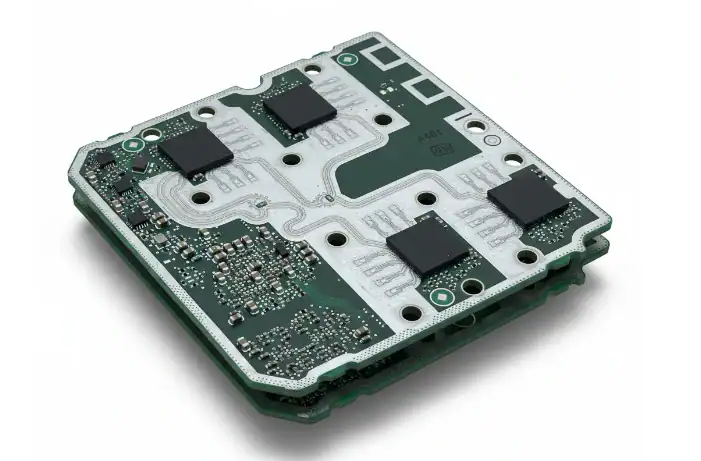
Start With The Components, Not The Board
Most people start by drawing a board outline and then cramming components into it. That’s backwards.
Your PCB size is determined entirely by the components you need to put on it. Start by compiling a complete list of every part, with their exact footprints from the official datasheet. Never trust the default footprints in your design software – I’ve seen more than one disaster caused by a library footprint that was 0.5mm too small.
Don’t forget to check component heights either. That tall electrolytic capacitor might fit perfectly on the board, but it will punch right through the top of your enclosure if you don’t account for it.
Clearance Rules That Will Save You From Disaster
Spacing isn’t optional. These are hard numbers that come from decades of manufacturing experience. Ignore them, and you’ll get solder bridges, overheating, and boards that fail right out of the box.
| Component Type | Minimum Clearance | Special Requirements |
|---|---|---|
| Standard SMDs | 0.2-0.5mm | Keep fine-pitch ICs away from connectors |
| Through-hole components | 1-2mm | Extra space for wave soldering |
| Power components | ≥3mm | For proper heat dissipation |
| High-voltage circuits | ≥8mm per 1000V | Follow IPC-2221 standards |
| Board edge | 2-3mm | No components or vias within this area |
If you’re wondering how these clearances affect the assembly process, read our previous guide: [What is PCB Assembly?]
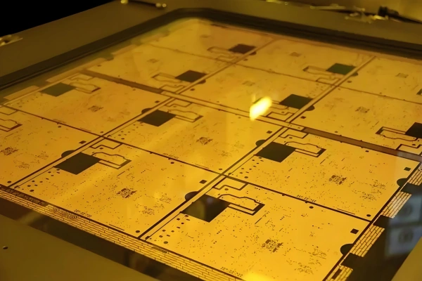
Traces, Vias, And The Hidden Space Eaters
Components aren’t the only things that take up space. Most beginners drastically underestimate how much room they need for routing.
A good rule of thumb: add 30% extra space to your initial component area just for traces and vias. That might seem like a lot, but you’ll be surprised how quickly it gets used up.
Standard via sizes work for most designs: 0.3mm hole diameter with 0.6mm pad. For high-density designs, you can go down to 0.2mm holes, but that will increase your manufacturing cost significantly.
The Enclosure Is The Final Judge
No matter how perfect your layout is, if it doesn’t fit in the enclosure, it’s useless.
Always get a 3D model of your enclosure before finalizing your PCB dimensions. Import it into your design software and do a complete fit check. Pay special attention to:
- Mounting hole positions and tolerances
- Connector alignment with cutouts
- Clearance for buttons and LEDs
- Any internal ribs or supports in the enclosure
And always add a 0.1-0.2mm tolerance gap around the entire board. Plastic enclosures shrink slightly during manufacturing, and metal enclosures have their own tolerances. A tight fit on paper will become an impossible fit in real life.
2026 Trend: AI Is Automating Dimension Optimization
Something game-changing is happening in PCB design software right now.
By the end of 2026, 65% of professional PCB designers will be using AI-powered dimension and panelization tools. These tools don’t just check for errors – they automatically optimize your board size to minimize waste and maximize panel utilization.
We’ve been testing one of these tools internally, and the results are impressive. It has increased our average panel utilization from 72% to 87%, which translates to an average 15% reduction in material costs for our clients. It also catches dimension conflicts that even experienced designers miss.
The days of manually arranging boards on a panel are coming to an end.
The #1 Costly Dimension Mistake
Poor panelization.
You could have the perfect board size, but if it doesn’t fit efficiently on a standard 18×24 inch production panel, you’ll be throwing money away.
For example, a 50x50mm board fits 40 pieces on a standard panel. A 51x51mm board only fits 36 pieces. That’s a 10% increase in cost per board, just for 1 extra millimeter.
Always check with your manufacturer about their standard panel sizes before finalizing your dimensions. A tiny adjustment can save you thousands in mass production.
Real Questions, Real Answers
Q: What is the smallest PCB size that can be manufactured?
A: For standard PCB manufacturing, the minimum practical size is about 5x5mm. Anything smaller than that becomes extremely difficult to handle during assembly. We can make smaller boards for special applications, but they require custom tooling and hand assembly, which increases cost dramatically.
Q: Why does my manufacturer keep asking me to increase my board size?
A: Because they’re trying to save you money. If your board size results in very low panel utilization, they will suggest a small adjustment that allows more pieces per panel. Most designers don’t realize that a 1mm increase in board size can actually decrease your per-unit cost by 20% or more.
If you’re finalizing your PCB design and want to make sure your dimensions are manufacturable and cost-effective, we’re here to help. Send us your Gerber files and enclosure drawings today, and we’ll do a free, no-obligation dimension check within 24 hours.
About US
Founded in 2012, JKRGLO strives to build a one-stop platform for the electronic industry chain. By integrating PCB manufacturing, component procurement and PCB assembly services, we enable digital PCBA processing. With increasing investment in innovation and digital systems, we have achieved rapid growth and emerged as a leading PCB and PCBA manufacturer in the industry, capable of rapidly producing high-reliability and cost-effective products.