
PCB Assembly Files: The 2-Second Mistake That Wrecks Your Entire Production Run
What files are needed for PCB assembly? You need 4 non-negotiable core documents: Gerber files, BOM (Bill of Materials), pick-and-place file, and assembly drawings. Missing any single one will delay your production by 3-7 days, and 60% of the time leads to boards that don’t work at all.
Why 90% Of Designers Waste Weeks On File Back-And-Forth
If you’ve ever spent 10 days emailing back and forth with a factory about “missing files” after you thought you sent everything, you’re not alone. Most designers spend months perfecting their circuit layout, then rush through the export process in 2 minutes. That’s where everything falls apart.
Factories don’t ask for extra files to be annoying. They ask because they literally cannot build your board correctly without them.
I saw this blow up spectacularly last year. A consumer electronics client sent us only their top-layer Gerber file for a smart watch motherboard. They swore “that’s all we ever send to our old factory”. We warned them we couldn’t proceed, but they insisted we “just figure it out”.
We didn’t figure it out.
They ended up paying $19,000 to scrap 3,000 half-assembled boards, and missed their Amazon Prime Day launch window entirely. All because they didn’t click “export all layers” in their design software.
The 4 Files That Actually Matter (And What Each One Does)
Forget the random extra files your design software spits out. Factories only care about these four. Nothing else matters.
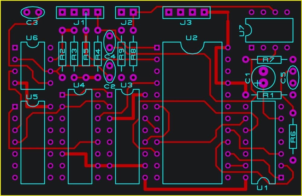
Gerber files are the DNA of your board. They tell the machines exactly where to etch copper, drill holes, apply solder mask, and print silkscreen. Here’s the secret no one tells you: Gerber is not one file. It’s a separate file for every single layer of your board. If you miss the drill layer, we can’t drill any holes. If you miss the solder mask layer, your entire board will be bare copper.
The BOM is your shopping list. It tells us which components to buy, how many, and from whom. This is the most important file you will ever send. A single typo in a part number – changing a 0 to an O, or a 1 to an I – will result in the wrong part being soldered to every single board.
The pick-and-place file is the instruction manual for the robots. It contains the exact X/Y coordinates and rotation angle for every component on the board. Without this file, we have to place every part by hand. That increases your cost by 12x and turns a 3-day production run into a 3-week nightmare.
Assembly drawings are the fine print. They cover everything else: which components are polarized, which need to be hand-soldered, how tight to torque the connectors, and any special testing requirements. If you need a capacitor mounted 2mm above the board for heat dissipation, this is where you tell us.
If you’re still unclear about how these files translate into physical boards on the factory floor, read our previous guide: [What is PCB Assembly?]
What We Actually Need Vs. What You Think We Need
This table will eliminate 90% of the email threads between you and your manufacturer.
| File Type | Exact Requirements | Most Common Idiotic Mistake | What Happens When You Mess Up |
|---|---|---|---|
| Gerber Files | All layers (top/bottom copper, solder mask, silkscreen, drill, outline) | Sending only the top copper layer | We cannot build your board. Period. |
| BOM | Full manufacturer part number, quantity, footprint, value | Using internal part codes like “CAP-100NF-0402” | We guess the wrong part. You pay for rework. |
| Pick-and-Place File | CSV/TSV with X, Y, rotation, and reference designator | Sending a screenshot of your layout | Components are placed backwards or in the wrong spot. |
| Assembly Drawings | PDF with polarity marks and special notes | No drawings at all | Polarized capacitors explode. Diodes are soldered backwards. |
2026 Trend: AI Is Killing The File Nightmare
Something long overdue is finally happening in our industry.
By the end of 2026, 82% of professional PCB assembly facilities will have deployed AI-powered pre-production file validation systems. These systems will automatically check for missing layers, BOM typos, footprint mismatches, and design for manufacturing (DFM) errors before a human ever looks at your files.
The days of waiting 4 days for the factory to tell you that you forgot the bottom silkscreen layer are over.
The #1 File Mistake That Costs The Most Money
Using internal part numbers in your BOM.
I cannot yell this loud enough. If your BOM says “RES-1K-0603” instead of “Panasonic ERJ-6ENF1001V”, we have no idea what part you want. We will have to email you. You will take 2 days to respond. We will lose our spot in the production queue. Your lead time will double.
And if we guess wrong? You get 5,000 boards with the wrong resistors, and you pay to throw them all away. Always use full, official manufacturer part numbers. No exceptions. No shortcuts.
Real Questions, Real Answers
Q: Why can’t I just send you my KiCad/Altium project file? That has everything in it.
A: You can, but you shouldn’t. First, version compatibility is a disaster. We’ve had clients send Altium 25 files that our Altium 24 software can’t open, and vice versa. Second, sending your full project file exposes your entire design to intellectual property theft. Third, Gerber/BOM/pick-and-place is the universal standard that every factory on Earth understands. Stick with it.
Q: My old factory never asked for all these files. Why do you?
A: Because your old factory was cutting corners. They were guessing at component values, skipping tests, and hoping for the best. That’s why you probably had a 20% failure rate and never knew why. We ask for all these files because we want to build your boards correctly the first time, not fix them later.
If you’re tired of spending weeks arguing with factories about missing files, we’re here to help. Send us your design files today, and we’ll run a completely free, no-obligation file check within 24 hours. We’ll tell you exactly what’s missing, what needs to be fixed, and give you a transparent, all-inclusive assembly quote.
No hidden fees. No last-minute surprises. No endless email threads. Just boards that work, built on time, every time.
About US
Founded in 2012, JKRGLO strives to build a one-stop platform for the electronic industry chain. By integrating PCB manufacturing, component procurement and PCB assembly services, we enable digital PCBA processing. With increasing investment in innovation and digital systems, we have achieved rapid growth and emerged as a leading PCB and PCBA manufacturer in the industry, capable of rapidly producing high-reliability and cost-effective products.