
PCB Manufacturing Process: Complete Step-by-Step Guide (2026 Updated)
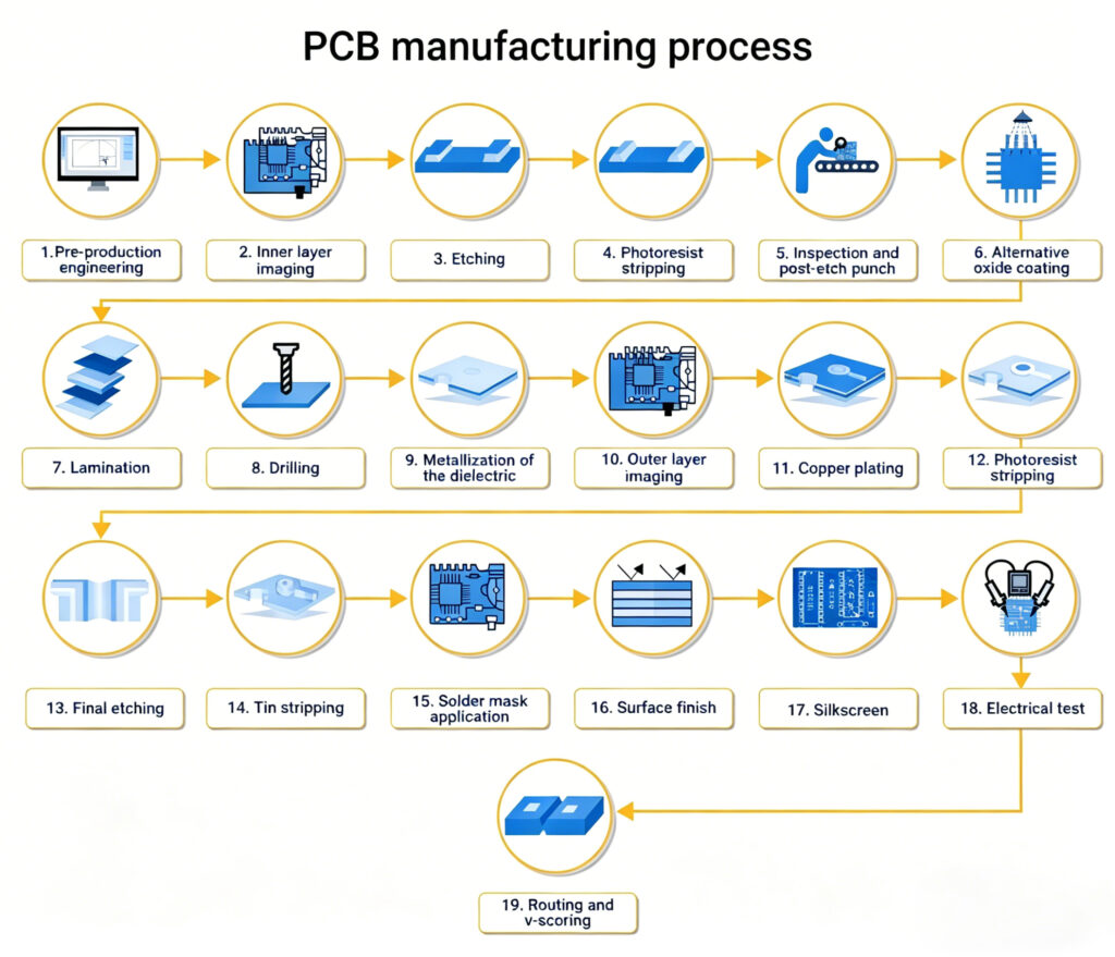
Pre-Production Engineering (The Most Overlooked Step)
- DFM (Design for Manufacturing) Check: We identify potential errors that will cause production failures, such as insufficient trace spacing, undersized annular rings, or invalid drill sizes.
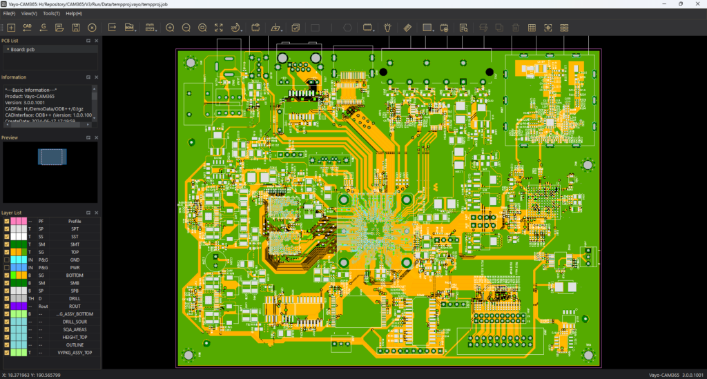
- CAM Processing: We convert your electronic files into machine-readable instructions, verify layer order, and run design rule checks (DRC).
- Production File Generation: We create drill programs, imaging layers, solder mask files, route files, and IPC netlists.
Production Line Truth: 80% of PCB production problems originate here. Cheap suppliers will skip the full DFM check and only verify file formats. If they make a mistake, they’ll blame your design instead of taking responsibility.
Inner Layer Imaging
- Photoresist Application: We apply a uniform layer of light-sensitive dry film to the copper surface.
- Laser Direct Imaging: A computer-controlled laser selectively hardens the photoresist to form your circuit pattern.
- Development: We wash away the unexposed photoresist with an alkaline solution, leaving the protected copper intact.
Pitfall Avoidance Guide: Old film-based imaging systems have a tolerance of ±0.1mm, while modern LDI systems achieve ±0.02mm. For high-speed designs or fine-pitch components, always confirm your supplier uses LDI.
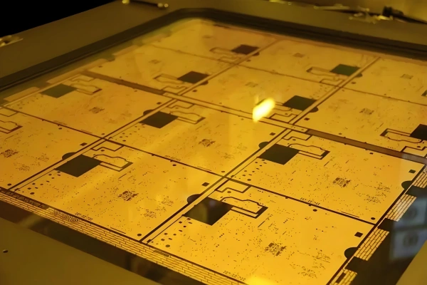
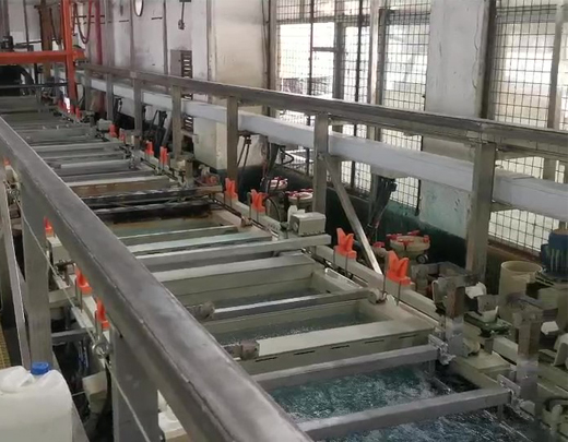
Etching
Etching removes the excess copper that isn’t protected by the hardened photoresist, revealing your exact circuit pattern.
We use a conveyorized develop-etch-strip line with controlled spray pressure and chemistry. Key parameters we monitor:
- Etchant temperature and concentration
- Panel movement speed
- Spray pressure distribution
Photoresist Stripping
We remove the remaining hardened photoresist using a caustic solution combined with high-pressure water rinsing. This exposes the pure copper circuit pattern underneath.
Inspection & Post-Etch Punch
This is the first major quality control checkpoint.
- Post-Etch Punch: We punch alignment holes using optical targets on the inner layers to ensure perfect layer-to-layer registration.
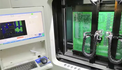
- Automated Optical Inspection (AOI): High-definition cameras scan every inch of the board to detect shorts, opens, trace width variations, and missing features.
Production Line Truth: Cheap suppliers will skip the AOI inspection for inner layers. Any defects here will be permanently sealed inside the board during lamination and impossible to repair later.
Alternative Oxide Coating
We apply a thin oxide coating to the copper circuit patterns. This acts as an adhesion promoter to ensure strong bonding between layers during lamination and prevents copper oxidation.
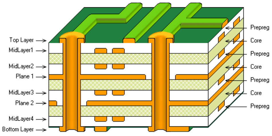
Lamination
Lamination bonds the inner layers, prepreg (sticky fiberglass), and copper foil into a single solid multilayer board.
The process:
- Stack-Up Preparation: We carefully arrange the layers in a symmetrical configuration according to your stack-up design.
- Hot Pressing: We apply 300-400 PSI of pressure at 180-200°C for 2 hours.
- Cold Pressing: We cool the stack under pressure to prevent warping.
Pitfall Avoidance Guide: To rush orders, some factories will cut the cure time to 45 minutes and crank up the temperature. This creates weak internal bonds that will delaminate when the board gets hot in use.
Drilling
We drill thousands of tiny holes for vias and component mounting using computer-controlled X-ray drill machines.
- Minimum drill diameter: 125 microns (0.0049 inches)
- Positioning accuracy: ±5 microns
- We remove all burrs from the hole walls after drilling.
Production Line Truth: Drill bits wear out. Reputable factories replace drill bits every 1,000 hits. Cheap factories reuse them up to 5,000 times, resulting in rough hole walls that cause plating failures.
Metallization of the Dielectric
This step makes the drilled hole walls conductive.
- De-Smear: We remove all epoxy residue from the hole walls using chemical or plasma etching.
- Catalyst Activation: We apply a palladium-based catalyst to initiate the copper deposition reaction.
- Electroless Copper Deposition: We deposit a uniform 20-micron thick copper layer on all surfaces, including the inside of the holes (per IPC Class 2 requirements).
Pitfall Avoidance Guide: This is the step 90% of cheap suppliers skip. They cut the de-smear time and dilute the chemicals, resulting in incomplete copper plating inside the holes. This causes intermittent open circuits that appear 6-12 months after production.
Outer Layer Imaging
We repeat the same photoresist and LDI process used for the inner layers, but this time for the outer layers of the board.
Copper Plating
We electroplate additional copper onto the surface and inside the holes to ensure reliable electrical connectivity between layers.
After copper plating, we apply a thin layer of tin to protect the copper pads and traces during the final etching process.
Photoresist Stripping (Outer Layer)
We remove the photoresist from the outer layers, exposing the unwanted copper that will be etched away.
Final Etching
We chemically remove the exposed unwanted copper using an ammoniacal etchant. The tin layer protects the desired copper circuit pattern from being etched.
Tin Stripping
We dissolve the protective tin layer using concentrated nitric acid, revealing the final clean copper circuit pattern.
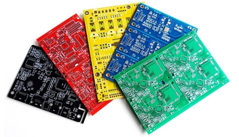
Solder Mask Application
Solder mask provides electrical insulation, prevents solder bridges, and protects the copper from corrosion. We use liquid photo imageable (LPI) solder mask for all boards.
- LPI coating
- UV imaging
- Developing
- Curing and final baking
Surface Finish
Complete Surface Finish Comparison (2026)
| Type | Description | Cost | Shelf Life | Best For | Common Pitfalls |
|---|---|---|---|---|---|
| OSP | Organic water-based coating | Lowest | 3-6 months | High-volume consumer electronics | Cannot be reworked multiple times |
| Lead-Free HASL | Hot air solder leveling | Low | 12 months | General purpose boards | Uneven surface, not suitable for fine pitch |
| ENIG | Electroless nickel immersion gold | Medium | 12-24 months | Fine pitch, BGA, high reliability | Black pad defect risk |
| ENEPIG | Nickel-palladium-gold | High | 24+ months | Automotive, medical, wire bonding | Higher cost |
| Immersion Silver | Thin silver coating | Medium | 6-12 months | High-speed designs | Tarnishes easily |
| Hard Gold | Thick gold plating | Highest | 24+ months | Edge connectors, high wear areas | Not suitable for soldering |
Silkscreen
Electrical Test (E-Test)
- 100% of boards are tested at JKR Precision
- We test every connection point on the board
- Any failed board is immediately scrapped
Routing & V-Scoring
- Routing: Leaves small tabs that are easily broken off
- V-Scoring: Cuts diagonal grooves on both sides of the panel for easy separation
2026 PCB Manufacturing Industry Updates
- AI-Powered AOI: AI inspection systems now catch 35% more fine-pitch defects than human inspectors, especially for traces under 0.1mm wide. All JKR production lines have been upgraded to AI AOI as of Q1 2026.
- EU CSRD Mandate: Starting in 2027, all electronic components sold in the EU require full digital traceability from raw material to finished product. We estimate 30% of small unregulated factories in China will shut down by the end of 2026 because they cannot afford the required upgrades.
Real Questions, Real Answers
Q: Why can one supplier quote $2 and another quote $6 for the exact same PCB design?
- Skip full DFM checks
- Reuse drill bits 5x longer than recommended
- Cut de-smear and plating times in half
- Only test 5% of your boards
- Use cheap solvent-based solder mask