
JKRGLO Advanced PCB Fab
HOME / Advanced PCB Fabrication
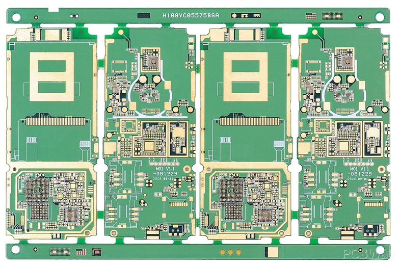
About Advanced PCB Fabrication
Advanced PCB Fabrication refers to high-precision, customized printed circuit board manufacturing services designed for high-end fields and demanding technical requirements. Different from standard PCBs, it adopts special substrate materials, sophisticated processes and strict parameter control to meet the high-performance needs of products in harsh or precision scenarios.
Our advanced PCB services integrate professional R&D support and strict quality management, providing reliable solutions for high-end electronic products that require high frequency, high temperature resistance, high precision and anti-interference.
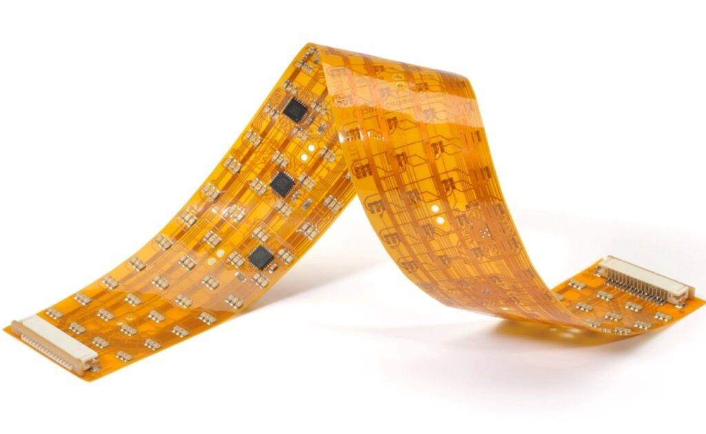
FLEXIBLE PRINTED CIRCUIT BOARDS
Flexible PCBs (FPCs) are crafted from flexible substrates like polyimide (PI), enabling bending and fitting into compact or curved spaces. Unlike rigid PCBs, FPCs adapt to product shapes (no need to design products around the board). Available in single-layer, multi-layer or dynamic flex designs, they support unique, lightweight electronic configurations and are ideal for space-saving modern devices.
BENEFITS
- Excellent resistance to temperature, chemicals, and radiation
- Lightweight and thin
- High reliability with fewer interconnects
- Compatible with diverse components and connectors
- Space-saving design
- Reduces packaging and material costs
- Minimizes assembly errors and repair needs
- Supports complex, dynamic applications
Flexible PCB Capability
| Feature | Capability |
| Quality Grade | Standard IPC 2 |
| Number of Layers | 1 - 8layers |
| Order Quantity | 1pc - 10000+pcs |
| Build Time | 2days - 5weeks |
| Material | DuPont PI, Domestic Shengyi PI |
| Board Size | Min 6*6mm, Max 406*610mm |
| Board Thickness | 0.1mm - 0.8mm |
| Copper Weight (Finished) | 0.5oz - 2.0oz |
| Min Tracing/Spacing | 3mil/3mil |
| Solder Mask Sides | As per the file |
| Solder Mask Color | Green, White, Blue, Black, Red, Yellow |
| Solder-stop coating---Soldermask oil | Green, White, Blue, Black, Red, Yellow |
| Solder-stop coating---Coverlay | PI and PET film |
| Silkscreen Sides | As per the file |
| Silkscreen Color | White, Black, Yellow |
| Surface Finish | HASL - Hot air solder leveling |
| Lead - free HASL - RoHS | |
| ENIG - RoHS | |
| Immersion Tin - RoHS | |
| OSP - RoHS | |
| Min Annular Ring | 4mil |
| Min Drilling Hole Diameter | 8mil |
| Min. hole size---Drilling (PTH) | 0.2mil |
| Min. hole size---Punching (NPTH) | 0.5mil |
| Tolerance of dimension | ±0.05mm |
| Other Techniques | Peelable solder mask |
| Gold fingers | |
| Stiffener (only for PI/FR4 substrate) |
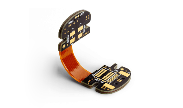
RIGID-FLEX PRINTED CIRCUIT BOARDS
Rigid-flex PCBs combine the advantages of rigid and flexible PCBs, integrating flexible circuit sections with rigid board areas. These hybrid circuits feature multi-layer conductive layers separated by rigid/flexible insulation materials, with plated through-holes connecting all layers. The design supports 3D configurations, enabling bending while maintaining mechanical stability in key areas.
BENEFITS
- Ideal for dynamic bending and 3D assemblies
- High integration for complex designs
- Fewer connectors and solder joints for increased reliability
- Excellent performance in harsh environments
- Easy to test and maintain
- Improved product lifespan
- Space-saving and compact structure
- Supports high-density interconnects
Rigid-Flex PCB Capability
| Feature | Capability |
| Quality Grade | Standard IPC 2 |
| Number of Layers | 2 - 24layers |
| Order Quantity | 1pc - 10000+pcs |
| Build Time | 2days - 5weeks |
| Material | DuPont (PI25UM), FR4 |
| Board Size | Min 6mm x 6mm / Max 457mm x 610mm |
| Board Thickness | 0.6mm - 5.0mm |
| Copper Weight (Finished) | 0.5oz - 2.0oz |
| Min Tracing/Spacing | 3mil/3mil |
| Solder Mask Sides | As per the file |
| Solder Mask Color | Green, White, Blue, Black, Red, Yellow |
| Silkscreen Sides | As per the file |
| Silkscreen Color | White, Black, Yellow |
| Surface Finish | HASL - Hot air solder leveling |
| Lead - free HASL - RoHS | |
| ENIG - RoHS | |
| Min Annular Ring | 4mil |
| Min Drilling Hole Diameter | 8mil |
| Impedance control | ±10% |
| Other Techniques | HDI |
| Gold fingers | |
| Stiffener (only for PI/FR4 substrate) |
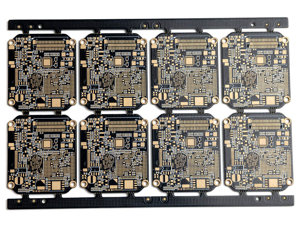
HIGH DENSITY INTERCONNECT (HDI) PRINTED CIRCUIT BOARDS
HDI PCBs boast higher wiring density, ideal for compact, high-performance electronic designs. With advanced technologies (microvias, blind vias, buried vias), they enable faster signal transmission, enhanced reliability and product miniaturization. Widely used in aerospace, military, telecommunications, consumer electronics and medical devices— the high-end industries demanding strict space, performance and precision standards.
BENEFITS
- Improved Signal Integrity
- Higher Component & Connection Density
- Smaller Size, Lighter Weight
- Cost Optimization & Design Flexibility
- Greater Reliability & Thermal Performance
- Faster Time-to-Market
- Lower Inductance, Capacitance & EMI
Our Available HDI PCB Structures
| HDI Structures | Type of Micro vias | Mass Production | Small-Middle Batch | Prototype | Available |
| 1+N+1 | Blind vias | Yes | Yes | Yes | 4 layers+ |
| 2+N+2 | Blind/Buried staggered vias | Yes | Yes | Yes | 6 layers+ |
| 2+N+2 | Blind/Buried stacked vias | Yes | Yes | Yes | 6 layers+ |
| 3+N+3 | Blind/Buried staggered vias | / | Yes | Yes | 8 layers+ |
| 3+N+3 | Blind/Buried stacked vias | / | / | Yes | 8 layers+ |
HDI PCB Capability
| Feature | Capability |
| Quality Grade | Standard IPC 2 |
| Number of Layers | 4 - 24layers |
| Order Quantity | 1pc - 10000+pcs |
| Build Time | 2days - 5weeks |
| Material | FR4 standard Tg 140°C,FR4 High Tg 170°C, FR4 and Rogers combined lamination |
| Board Size | Min 6*6mm / Max 457*610mm |
| Board Thickness | 0.4mm - 3.0mm |
| Copper Weight (Finished) | 0.5oz - 2.0oz |
| Min Tracing/Spacing | 2.5mil/2.5mil |
| Solder Mask Sides | As per the file |
| Solder Mask Color | Green, White, Blue, Black, Red, Yellow |
| Silkscreen Sides | As per the file |
| Silkscreen Color | White, Black, Yellow |
| Surface Finish | HASL - Hot Air Solder Leveling |
| Lead Free HASL - RoHS | |
| ENIG - Electroless Nickle/Immersion Gold - RoHS | |
| Immersion Silver - RoHS | |
| Immersion Tin - RoHS | |
| OSP - Organic Solderability Preservatives - RoHS | |
| Min Annular Ring | 4mil, 3mil - laser drill |
| Min Drilling Hole Diameter | 6mil, 4mil - laser drill |
| Max Exponents of Blind/Buried Vias | stacked vias for 3 layers interconnected, staggered vias for 4 layers interconnected |
| Other Techniques | Flex-rigid combination |
| Via In Pad | |
| Buried Capacitor (only for Prototype PCB total area ≤1m²) |
ALUMINUM PRINTED CIRCUIT BOARDS
Aluminum PCBs (most common MCPCBs) are renowned for excellent thermal management. With an aluminum core, standard FR4 and a thermally conductive layer, they dissipate heat efficiently to boost component cooling and overall performance. Ideal for high-power, tight-tolerance applications—LED lighting, automotive systems, power electronics.
BENEFITS
- Efficient Thermal Dissipation
- High Reliability
- Improved Performance
- Power Handling
- Mechanical Durability
- Cost-Effective Solution
The able below features some of our aluminum core materials.
| Items | Performance Index (Measured value) |
| Peeling strength (n/mm) | 1.8 |
| Insulation resistance (ω) | >1*10 g |
| Breakdown voltage (vdc) | >2 k |
| Soakable soldering (°C/m) | 280°C / 260°C, 1 min, no bubble & delamination |
| Thermal conductivity (ω/m-k) | >0.8 |
| Thermal resistance (°C/ω) | < 1.2 |
| Combustibility | fv-o |
| Dielectric constant (1mhz) | 4 |
| Dielectric loss angle (tangent) | 0.03 |
Aluminum core PCB manufacturing capabilities
| Feature | Capability |
| Quality Grade | Standard IPC 2 |
| Number of Layers | 4 - 24layers |
| Order Quantity | Order Quantity |
| Build Time | 2days - 5weeks |
| Material | Aluminum core (Domestic 1060), Copper core, FR4 covering |
| Board Size | Min 6*6mm | Max 610*610mm |
| Board Thickness | 0.8mm - 5.0mm |
| Copper Weight (Finished) | 0.5oz - 10.0oz |
| Min Tracing/Spacing | 4mil/4mil |
| Solder Mask Sides | As per the file |
| Solder Mask Color | Green, White, Blue, Black, Red, Yellow |
| Silkscreen Sides | As per the file |
| Silkscreen Color | White, Black, Yellow |
| Surface Finish | HASL - Hot Air Solder Leveling |
| Lead Free HASL - RoHS | |
| ENIG - Electroless Nickle/Immersion Gold - RoHS | |
| Min Annular Ring | 4mil |
| Min Drilling Hole Diameter | 6mil |
| Other Techniques | Countersink holes |
| Screw holes |
HIGH FREQUENCY PRINTED CIRCUIT BOARDS
High Frequency PCBs are designed for high-speed, high-frequency signal transmission typically in the range
of 500MHz to 2GHz. These boards are essential for applications in RF (radio frequency), microwave, and
mobile communications, where signal integrity and transmission speed are critical. Unlike standard PCBs,
high-frequency boards require specialized materials like Rogers laminates to maintain stable electrical
performance and ensure minimal signal loss. Their design demands tight control over parameters such as
dielectric constant (Er), conductor width, and spacing, making precision fabrication crucial.
BENEFITS
- Faster Signal Transmission
- Improved Signal Integrity
- Specialized Material Support
- High Customization & Flexibility
- Advanced Applications
- Reliable & Scalable Production
Commonly Used Materials for High-Frequency PCBs
| Material | Dielectric Constant |
| RO4350B | 3.48±0.05@10 GHz |
| RO4003C | 3.38±@10 GHz |
| Ro3003 | 3.00±0.04@10 GHz |
| Ro3010 | 10.2±0.03@10 GHz |
| RT5880 | 2.20±0.02@10 GHz |
High-Frequency PCB manufacturing capabilities
| Feature | Capability |
| Quality Grade | Standard IPC 2 |
| Number of Layers | 2 - 24layers |
| Order Quantity | 1pc - 10000+pcs |
| Build Time | 2days - 5weeks |
| Material | RO4003C, RO4350B, Ro3003, Ro3010, RT5880 |
| PP | Rogers 4450F, Domestic-(25FR), Domestic-(RF-27), Domestic-(6700) |
| Board Size | Min 6mm x 6mm | Max 457mm x 610mm |
| Board Thickness | 0.4mm - 5.0mm |
| Copper Weight(Finished) | 0.5oz - 2.oz |
| Min Tracing/Spacing | 3mil/3mil |
| Solder Mask Sides | As per the file |
| Solder Mask Color | Green, White, Blue, Black, Red, Yellow |
| Silkscreen Sides | As per the file |
| Silkscreen Color | White, Black, Yellow |
| Surface Finish | Electroless nickel/immersion gold (ENIG) - RoHS |
| Immersion silver - RoHS | |
| Immersion tin - RoHS | |
| Organic solderability preservatives - RoHS | |
| Min Annular Ring | 4mil |
| Min Drilling Hole Diameter | 6mil |
| Impedance tolerance | ±10% |
| Other Techniques | Peelable solder mask |
| Gold fingers | |
| Carbon oil | |
| Countersink holes |