
JKRGLO PCB Prototype Service
HOME / PCB Prototype
What is PCB Prototype?
PCB Prototype is the small-batch trial production of PCBs in the product R&D stage, used to verify circuit design feasibility, debug errors and optimize schemes before mass production. It features small volume, fast delivery and customizable processes, serving as the key link between PCB design and mass production.
We specialize in custom PCB prototype manufacturing, balancing high precision with efficient turnaround. Our services are adaptable to various R&D scenarios, empowering our customers to quickly complete prototype validation and accelerate the commercialization of their new products.
Our PCB Prototype Service
PCB Prototype Types
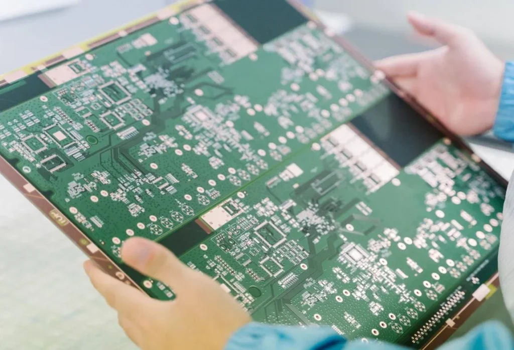
Bare PCB Prototyping: Only blank PCBs manufactured, without any electronic components. Ideal for customers who solder components themselves.
PCBA Prototyping: One-stop fabrication of bare PCBs with SMT placement/THT through-hole insertion. Time-saving & efficient, ready for immediate testing.
Rush PCB Prototyping: Priority order scheduling for urgent R&D validation needs (Fastest delivery in 24 hours).
Processes & Specification Range
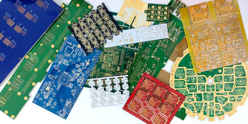
Substrate Types: Supports FR-4 (Standard), high-frequency substrates, high-temperature substrates and other special substrates.
Layer Count Range: 1-8 Layers
Build Time: 1 – 7 days
Supported File Formats: Gerber, PCB, DXF and other design file formats, with professional file verification assistance.
PCB Prototype Capabilities
| Features | Capability |
| Quality Grade | Standard IPC 1 |
| Order Quantity | 5pcs - 100pcs |
| Build Time | 1 - 7 days |
| Material | Supports FR-4 (Standard), high-frequency substrates, high-temperature substrates and other special substrates. |
| Board Size | Min 6*6mm | Max 500*500mm |
| Board size tolerance | ±0.1mm - ±0.3mm |
| Board Thickness | 0.4mm - 2.0mm |
| Board Thickness Tolerance | ±0.1mm - ±10% of thickness of board |
| Copper Weight | 1.0oz - 2.0oz |
| Inner Layer Copper Weight | 0.5oz - 1.0oz |
| Copper Thickness Tolerance | +0μm +20μm |
| Min Tracing/Spacing | 5mil/6mil (copper weight: 1oz) |
| 8mil/8mil (copper weight: 2oz) | |
| Solder Mask Sides | As per the file |
| Solder Mask Color | Green, White, Blue, Black, Red, Yellow |
| Silkscreen Sides | As per the file |
| Silkscreen Color | White, Black |
| Surface Finish | Lead Free HASL - RoHS |
| HASL - Hot Air Solder Leveling | |
| ENIG - Electroless Nickle/Immersion Gold - RoHS | |
| Min Annular Ring | 5mil |
| Min Drilling Hole Diameter | 8mil |
| Min Width of Cutout (NPTH) | 0.8mm |
| NPTH Hole Size Tolerance | ±.002" (±0.05mm) |
| Min Width of Slot Hole (PTH) | 0.6mm |
| PTH Hole Size Tolerance | ±.003" (±0.08mm) - ±.006" (±0.15mm) |
| Surface/Hole Plating Thickness | 20μm - 30μm |
| SM Tolerance (LPI) | .003" (0.075mm) |
| Aspect Ratio | 10:1 (board thickness: hole size) |
Our PCB Prototype Advantages
Efficient Delivery: Standard prototyping delivered in 1-7 days, rush orders within 24 hours. No delays to your R&D progress.
Controllable Precision: Strictly compliant with IPC standards. Every prototype board undergoes electrical testing, eliminating short circuits, cold solder joints and other defects.
Flexible Customization: Supports small-batch production (MOQ 1 unit), special processes (ENIG, OSP) and custom-shaped PCB customization, suitable for all R&D scenarios.
Applicable R&D Fields
Why choose JKRGLO?
Save Time and Money in the Long Run With PCB Rapid Prototyping Services from JKRGLO
PCB prototyping is the best practice method used world-wide to verify the quality of a design before proceeding. In the past, some companies may not have had time to develop a prototype PCB, wait for the assembler to put that PCB prototype together and then test it. However, thanks to the rapid PCB prototyping offered by JKRGLO, this is no longer an issue. You can send in your prototyping PCB board design and have a fast PCB prototype in a week or less, giving you plenty of time to test your PCB proto board to fully prepare for your regular production run.