
PCB Silkscreen: A Comprehensive Guide for Designers and Manufacturers
The silkscreen layer is the final and most visible layer in PCB manufacturing, serving as the “visual guide” for anyone working with the circuit board. This layer consists of non-conductive epoxy ink markings that identify components, test points, symbols, logos, and critical safety information. For designers, manufacturers, and technicians, a well-designed silkscreen streamlines assembly, simplifies troubleshooting, and ensures compliance with industry standards. In this article, we’ll dive into the fundamentals of PCB silkscreen, key design considerations, practical optimization tips, common manufacturing methods, and essential guidelines to ensure your silkscreen is both functional and manufacturable.
What Exactly is PCB Silkscreen?
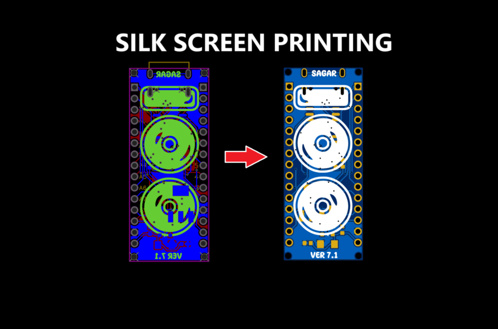
Imagine a toolbox with no labels on its drawers—you’d spend hours searching for the right tool. PCB silkscreen serves the same purpose as those labels: it provides clear, human-readable information that transforms a plain circuit board into an understandable and usable component. Also known as the “legend” layer, silkscreen is applied on top of the solder mask (the green, black, or other colored layer that protects the PCB’s copper traces) and includes text, symbols, and graphics that identify every critical part of the board.
Silkscreen ink is specially formulated to be non-conductive, heat-resistant, and durable enough to withstand the soldering process and long-term use. The most common ink colors in the industry are white and black, chosen for their high contrast against standard solder mask colors (e.g., white ink on green solder mask, black ink on white solder mask). While PCB design software like Altium Designer and KiCad offers standard fonts for silkscreen, designers have the flexibility to use custom fonts or logos—provided they meet manufacturing constraints. Silkscreen is typically applied using UV liquid photo-imaging (LPI) or direct legend printing (DLP), depending on the required precision and board complexity.See the full comprehensive guide, how PCB are manufactured in JKRGLO fab.
What Information Belongs on a PCB Silkscreen?
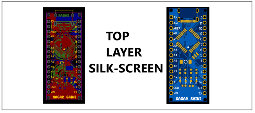
A well-designed silkscreen should include all information necessary for manufacturing, assembly, testing, and maintenance. Here’s a breakdown of the key elements to include:
- Company logos, designer names, or manufacturer identifiers to establish brand identity and traceability.
- Safety warnings and symbols, such as “High Voltage” (⚡) or “Caution: Static Sensitive” (ESD), to prevent accidents during handling.
- Version numbers (e.g., Ver1.0, V2.1, Rev A2) to track design iterations and ensure compatibility with components or assemblies.
- Test points (labeled as TP1, TP2, etc.) to facilitate electrical testing and troubleshooting during production.
- Component designators and polarity indicators (e.g., resistor R1, capacitor C5, diode polarity marks) to guide accurate assembly.
- Connector pinouts (for pin headers, USB ports, or other interfaces) to clarify wiring and functionality.
- Regulatory and compliance markings, such as RoHS, FCC, CE, or UL symbols, to demonstrate adherence to global safety and environmental standards.
On dense, miniaturized PCBs, space is limited, and it’s often impossible to include every piece of information. In such cases, prioritization is key—and we’ll cover how to optimize your silkscreen for compact designs later in this guide.
Industry-Standard Compliance Markings
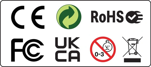
Regulatory markings are non-negotiable for commercial and consumer PCBs, as they indicate the product meets specific safety, environmental, and performance standards. Common markings include:
- RoHS: Indicates compliance with the EU Restriction of Hazardous Substances directive, which limits the use of lead, mercury, and other harmful materials. While RoHS has no mandatory symbol, the “RoHS” text or a green checkmark is widely used in the industry.
- CE: A self-declaration mark indicating compliance with EU directives (e.g., EMC, LVD). The CE letters must be equal in height (minimum 1.2mm if space is limited) with a small gap between them.
- UL: Signifies the PCB is manufactured by a UL-certified facility, adhering to safety standards like UL 796 and UL 94. The UL mark must include the UL logo and a control number (e.g., E123456).
- FCC: Required for electronic devices sold in the U.S., indicating compliance with electromagnetic interference (EMI) standards.
These markings not only ensure legal compliance but also build trust with customers and regulatory bodies.
How to Clean Up and Optimize Silkscreen for Dense PCBs
As PCBs become smaller and more compact, silkscreen overlap (e.g., component designators covering pads or vias) becomes a common issue. To resolve this, you’ll need to clean up your silkscreen while maintaining its functionality. Here’s a step-by-step prioritization framework to follow:
- Regulatory Requirements First: Prioritize RoHS, lead-free, and safety markings—these are non-negotiable and must be clear and unobstructed.
- Manufacturer Identification: Include PCB serial numbers, logos, and version numbers to enable traceability and quality control.
- Assembly Aids: Prioritize polarity marks, component placement indicators, and connector pinouts—these are critical for accurate assembly.
- Component Designators: Keep essential designators (e.g., for large or critical components) and remove or relocate redundant ones. If space is tight, use abbreviations or smaller fonts (within manufacturing limits).
- Test Points and Jumpers: Label test points and jumper locations only if they’re needed for production testing or maintenance.
Additional tips for optimization: Avoid placing silkscreen over pads, vias, or exposed copper traces (this can cause soldering issues or short circuits). If designators must be placed near components, position them slightly away to prevent overlap. Use simple, sans-serif fonts for readability, and ensure the font height and line width meet manufacturer requirements.
Common Methods for Creating PCB Silkscreen
There are three primary methods for applying silkscreen to PCBs, each with its own advantages, disadvantages, and ideal use cases. The choice depends on factors like board complexity, precision requirements, and production volume.
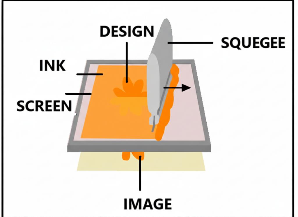
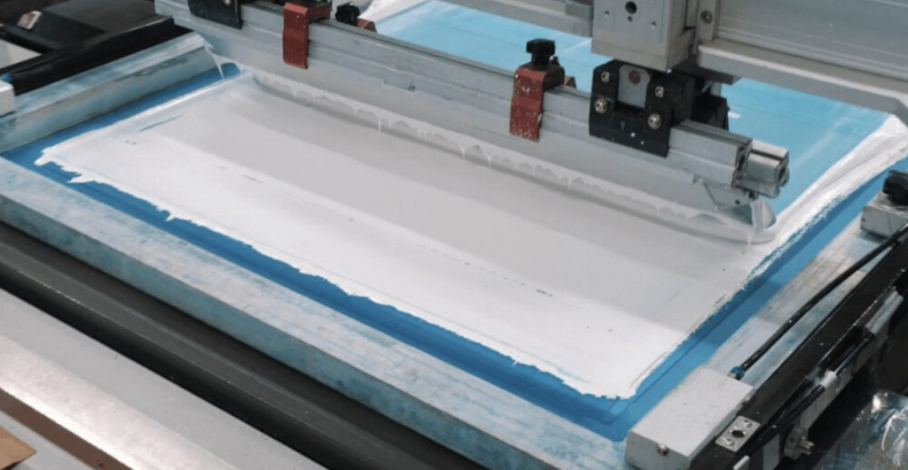
1. Screen Printing
Screen printing is the most widely used method for PCB silkscreen, especially for high-volume production. It involves using a fine mesh screen (stencil) to transfer ink onto the PCB surface. A squeegee is used to push the ink through the screen, creating the desired markings. This method is cost-effective for simple to moderately complex designs but may lack precision for very small text or dense boards.
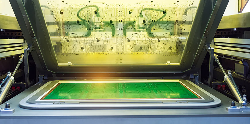
2. Liquid Photo Imaging (LPI)
LPI is a high-precision method ideal for dense, high-tech PCBs (e.g., those used in smartphones or medical devices). A photosensitive liquid epoxy ink is applied to the PCB, then exposed to UV light through a film that contains the silkscreen design. The unexposed ink is washed away, leaving behind fine, detailed markings. While LPI offers excellent resolution, it is more time-consuming and costly than screen printing due to the additional UV exposure and development steps.
3. Direct Legend Printing (DLP)
DLP uses inkjet printing technology to apply silkscreen directly onto the PCB, eliminating the need for stencils or UV exposure. This method is fast, accurate, and ideal for small-batch production or custom designs. DLP reduces manufacturing time and costs but may not match the high resolution of LPI or the durability of screen printing. It is best suited for PCBs that do not require extremely fine text or long-term harsh environment use.
The PCB Silkscreen Printing Process
Regardless of the method used, the core steps of silkscreen printing follow a consistent workflow, from design to final quality check. Here’s a detailed breakdown:
- Design Preparation: Create the silkscreen layer in your PCB design software (e.g., Altium, KiCad) and export it as a Gerber file—this file contains all the necessary information for the manufacturer to reproduce your silkscreen accurately. Ensure all text, symbols, and logos meet the manufacturer’s size and spacing requirements.
- Screen/Stencil Preparation: For screen printing, a stencil is created by applying a photosensitive emulsion to a mesh screen, then exposing it to light through a film of the silkscreen design. The unexposed emulsion is washed away, leaving a stencil of the desired markings. For DLP, no stencil is needed— the design is sent directly to the inkjet printer.
- Printing: The PCB is secured in place, and the ink is applied. For screen printing, a squeegee pushes ink through the stencil onto the PCB. For DLP, the inkjet printer applies ink directly to the board surface. For LPI, the liquid epoxy ink is applied evenly across the PCB before UV exposure.
- Curing: The printed PCB is exposed to UV light or heated to cure the ink, solidifying the markings and ensuring they adhere to the solder mask. Curing time varies depending on the ink type and method—typically 10-30 minutes for UV curing.
- Quality Check: The finished PCB is inspected to ensure the silkscreen is clear, accurate, and free of smudges, misalignments, or missing markings. Any defective boards are reworked or discarded to maintain quality standards.
Key Manufacturing Guidelines for PCB Silkscreen
To ensure your silkscreen is manufacturable and meets industry standards, follow these critical guidelines—based on best practices from leading PCB manufacturers like JKRGLO:
Spacing and Line Width
For optimal readability and manufacturability, the minimum line width (for text and symbols) and spacing between characters should be no less than 0.15mm (6mil). The minimum text height should be 1.0mm (40mil), with a preferred width-to-height ratio of 1:6. Smaller text or narrower lines may be difficult to print clearly and can lead to unreadable markings.
Overlapping and Prioritization
If silkscreen markings overlap with solder mask openings (e.g., pads or vias), manufacturers will prioritize the openings—meaning the silkscreen in that area will be omitted to avoid interfering with soldering. If you need silkscreen to remain over openings, be sure to note this in your order remarks so the manufacturer can accommodate your request.
Silkscreen on Aluminum PCBs
Aluminum PCBs (used for heat dissipation in LED and power electronics) support white and black silkscreen ink. White ink is recommended for green or black solder mask, while black ink is used for white solder mask. Avoid applying silkscreen to bare aluminum surfaces, as the ink adhesion is poor and will likely peel off over time.
Tolerance Specifications
Silkscreen markings may have minor deviations from the design, depending on the manufacturing method. The table below outlines permissible deviations (in mm) for different nominal length ranges and tolerance classes:
| Nominal Length Range (mm) | F (Fine) | M (Medium) | C (Coarse) | V (Very Coarse) |
|---|---|---|---|---|
| 0.5 up to 3 | ±0.2 | ±0.2 | ±0.4 | ±0.4 |
| Over 3 up to 6 | ±0.5 | ±0.5 | ±1.0 | ±1.0 |
| Over 6 | ±1.0 | ±1.0 | ±2.0 | ±2.0 |
About US
Founded in 2012, JKRGLO strives to build a one-stop platform for the electronic industry chain. By integrating PCB manufacturing, component procurement and PCB assembly services, we enable digital PCBA processing. With increasing investment in innovation and digital systems, we have achieved rapid growth and emerged as a leading PCB and PCBA manufacturer in the industry, capable of rapidly producing high-reliability and cost-effective products.