
PCB Board Design: A Beginner-Friendly Step-by-Step Tutorial
Printed Circuit Boards (PCBs) are the foundation of nearly all modern electronic devices, serving as a reliable platform to connect and power electronic components. For beginners, PCB design might appear daunting at first glance, but with a systematic approach and the right tools, it becomes an accessible and fulfilling skill. This blog will guide you through each stage of PCB design, from initial planning to final preparation for manufacturing, using a practical example to make the process easier to follow.
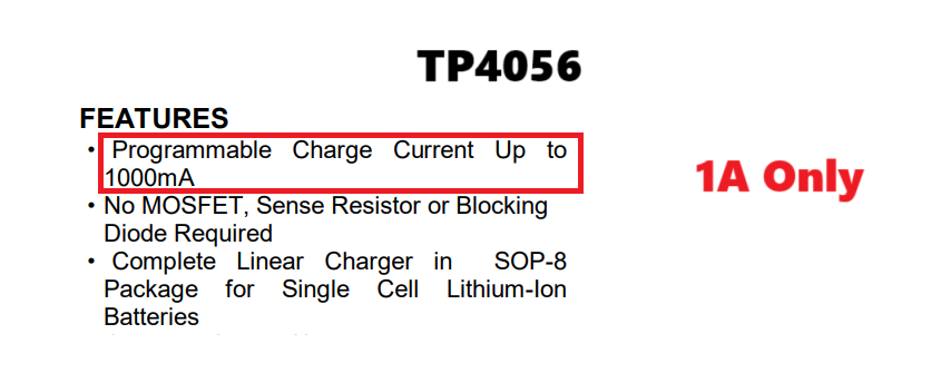
Today, we’ll walk through the design process of a lithium-ion battery charging module as our practical example. The TP4056 is a widely used charging module, but to enhance its current-carrying capacity, we’ll replace its core circuit with a new IC called IP2312—while keeping the PCB form factor similar to the TP4056. The IP2312 can deliver a charging current of up to 3A, making it more efficient for high-demand applications. For a detailed, in-depth tutorial on this specific design, check out our dedicated post.
Design Steps for Printed Circuit Board:
Step 1: Understand Your Circuit Requirements
Before you open any design software, it’s critical to have a clear understanding of the circuit you intend to build. Start by sketching a schematic on paper or using beginner-friendly software like KiCad, Eagle,EasyEDA . Include all essential components, such as resistors, capacitors, microcontrollers, and connectors, and ensure each component is correctly wired to guarantee the circuit functions as intended. Typically, circuit design begins with a hand-drawn sketch, inspired by real-world problems or needs. In our case, the problem we’re solving is the long charging time associated with the standard TP4056 module.
Step 2: Choose a PCB Design Software
For beginners, selecting PCB design software with an intuitive interface is key to a smooth learning experience. Popular options for beginners include KiCad, Eagle,EasyEDA —all of which allow you to create schematics, arrange components, and design the copper traces that connect them. These tools also offer extensive libraries of standard components, which simplifies the design process and saves time. To keep our tutorial straightforward, we’ll use EasyEDA throughout, thanks to its massive component library, user-friendly online platform, and comprehensive features.
Step 3: Create the Schematic
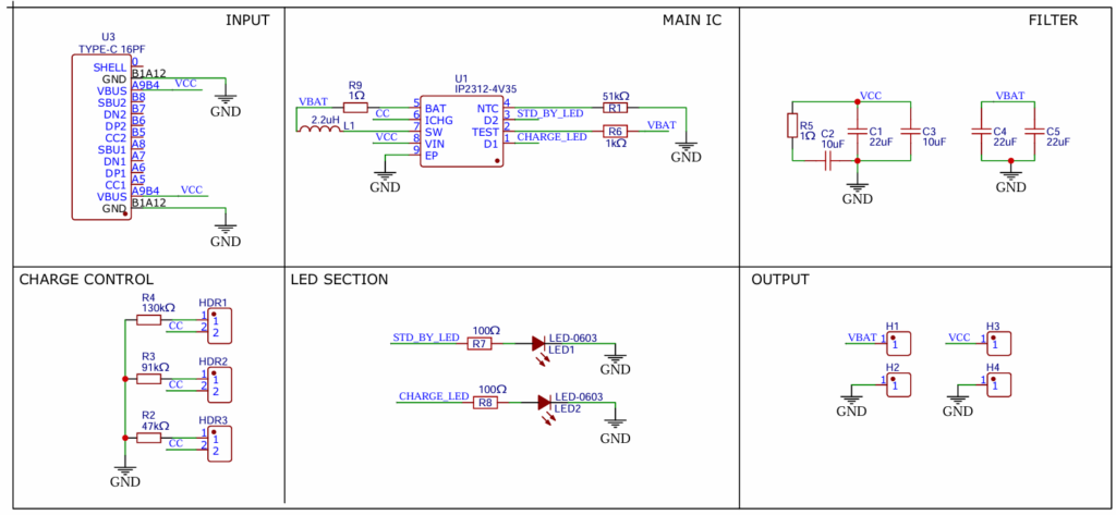
Once you’ve chosen your software, the next step is to create the schematic diagram. A schematic is a visual blueprint of the electrical connections, showing how each component interacts and connects to others. To create an accurate schematic, refer to the datasheet of your core IC (in our case, the IP2312) and arrange the components according to the recommended circuit configuration. Depending on your specific use case, you may need to adjust component values or types—there are often multiple alternatives for a single component to suit different requirements. The example schematic for our IP2312-based charging module is structured into distinct sections to improve readability and reduce research and development time.
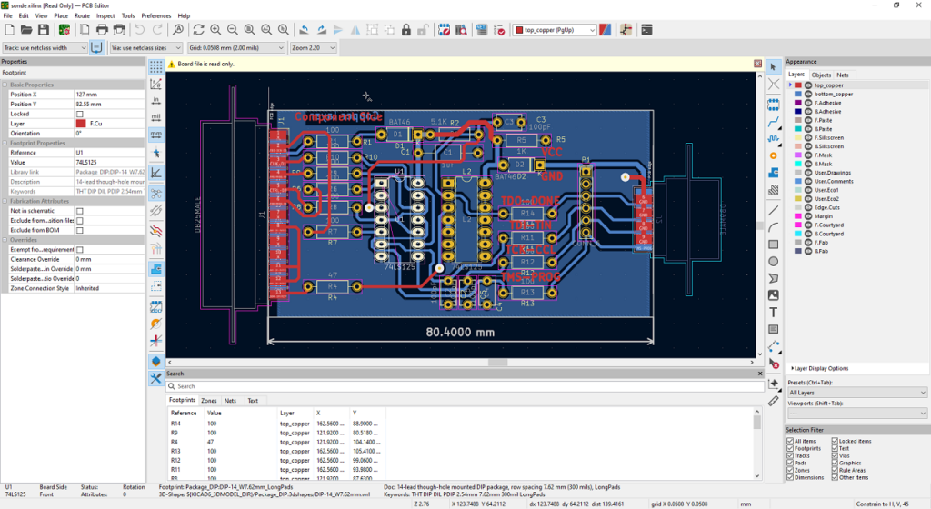
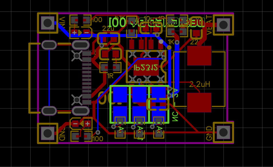
Step 4: Define the PCB Layout
After completing your schematic, it’s time to define the physical layout of your PCB. This stage involves several key steps to ensure optimal performance and manufacturability:
- Set the dimensions of the PCB board to fit your application (e.g., matching the form factor of the TP4056 in our example).
- Place components logically to minimize trace length, which helps reduce signal interference and improve performance.
- Ensure components with specific orientations—such as LEDs, connectors, or switches—are aligned correctly for practical use.
- Avoid overlapping components and leave enough clearance between them to facilitate soldering and prevent short circuits.
In our design, we placed all components close together to minimize trace length. Since we’re using the compact form factor of the TP4056, component orientation plays a crucial role in ensuring smooth routing and efficient use of space.
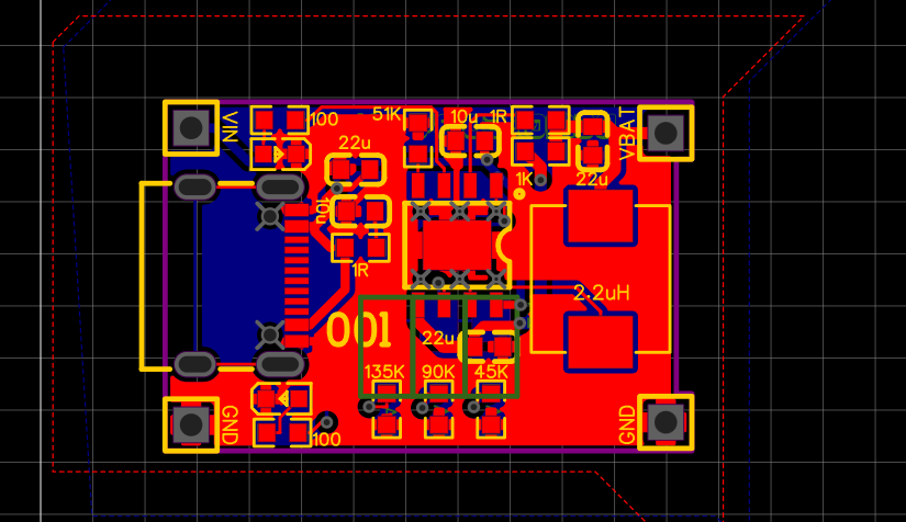
Step 5: Route Traces
Routing traces is the process of creating the copper paths that carry electrical signals between components on the PCB. Follow these essential guidelines to ensure reliable performance:
- Keep traces as short as possible to reduce resistance, capacitance, and electromagnetic interference (EMI).
- Route power and ground traces wider than signal traces to handle higher current and improve stability.
- Adhere to design rules, such as trace spacing, to avoid short circuits and ensure compliance with manufacturing standards.
- Use vias to connect traces on different layers if you’re designing a multi-layer PCB.
- Always consider the current rating and power dissipation of each trace—you can use online calculators to verify these values.
Most PCB design software offers an autorouting feature, which can save time during development. However, manual routing is often more reliable, as autorouting may not optimize for signal integrity or space efficiency.
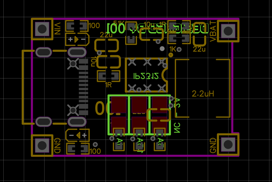
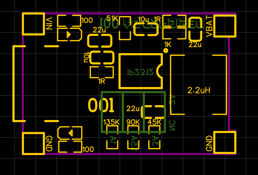
Step 6: Add Power and Ground Planes
For most PCBs—especially those handling significant current or sensitive signals—adding power and ground planes is essential. A power plane is a solid copper layer that distributes power evenly across the board, while a ground plane acts as a shield to reduce electrical noise and improve signal integrity. These planes are typically placed on entire layers of the PCB, providing a low-impedance path for current.
Since our design is a two-layer PCB, we added ground planes on both sides to minimize input voltage noise. This solid copper pour is connected to all ground traces in the circuit, creating a stable and reliable ground reference.
Step 7: Place Silkscreen and Other Markings
Add silkscreen labels to identify components, pin numbers, logos, or regulatory markings. The silkscreen layer is a vital part of PCB assembly and troubleshooting, as it helps technicians identify components and their correct placement. Ensure silkscreen text and symbols do not overlap with solder pads or traces, as this can interfere with soldering and functionality. For more detailed information on silkscreen design, check out our comprehensive guide on PCB silkscreen best practices.
Step 8: Verify with Design Rule Check (DRC)
Before finalizing your design, run a Design Rule Check (DRC) to identify any errors or violations. Common issues detected by DRC include incorrect trace spacing, unconnected traces, overlapping components, or insufficient clearance. Most PCB design software includes a built-in DRC tool, which ensures your design meets the manufacturer’s specifications and is ready for fabrication.
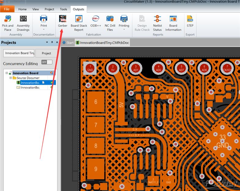
Step 9: Generate Gerber Files
Once your design is complete and verified with DRC, you need to export Gerber files. These files contain all the necessary information for PCB manufacturers to fabricate your board, including details of each layer (copper layers, silkscreen, solder mask, and solder paste). Each layer of your PCB is represented as a separate file in the Gerber set, ensuring the manufacturer can accurately reproduce your design.
Conclusion:
Once you have your Gerber files, you’re ready to submit them to a PCB manufacturer. Many manufacturers offer online quoting tools where you can upload your Gerber files, select board specifications (such as material, thickness, and solder mask color), and place your order with just a few clicks.
While PCB design may seem overwhelming at first, following these step-by-step instructions will help even beginners create functional, well-designed circuit boards. Remember, practice is key—over time, you’ll develop the skills to optimize layouts, minimize noise, and produce high-quality PCBs for your projects. Happy designing!
About US
Founded in 2012, JKRGLO strives to build a one-stop platform for the electronic industry chain. By integrating PCB manufacturing, component procurement and PCB assembly services, we enable digital PCBA processing. With increasing investment in innovation and digital systems, we have achieved rapid growth and emerged as a leading PCB and PCBA manufacturer in the industry, capable of rapidly producing high-reliability and cost-effective products.