
PCB Impedance Control: A Critical Guide to High-Speed Signal Integrity
Impedance represents the total opposition that an electrical circuit offers to the flow of alternating current (AC). It combines the effects of capacitance and inductance within the circuit, particularly at high frequencies, and is measured in Ohms—just like resistance. When impedance values across a circuit do not match, signal reflections and attenuation occur, directly degrading signal quality and leading to potential circuit malfunctions.
For modern high-frequency analog and digital circuits—especially those operating above 100 MHz—protecting the integrity of signals traveling along PCB traces is non-negotiable. At these frequencies, trace impedance becomes a critical factor; neglecting it can result in unexpected errors that are notoriously difficult to diagnose and resolve. Fortunately, impedance control provides PCB designers and manufacturers with a reliable way to manage these issues and ensure consistent signal performance.
What is Impedance Control and Signal Matching?
Impedance control involves aligning the dimensions and placement of PCB traces with the electrical properties of the substrate material, ensuring that signals remain noise-free and unattenuated during transmission. In high-speed designs, PCB traces can no longer be treated as simple point-to-point connections—they must be viewed as transmission lines. Impedance matching, a key part of this process, minimizes or eliminates signal integrity issues by ensuring that the impedance of the trace matches the impedance of the driver, receiver, and other components in the circuit. By following best practices in impedance control, designers can avoid or mitigate most common signal integrity problems.
In this blog, we’ll explore the importance of impedance control, the root causes of signal integrity issues, and practical strategies to achieve reliable impedance matching in PCB design.
Factors Determining Transmission Line Impedance
Typically, trace impedance in PCB design ranges from 25 to 125 Ohms, and it is influenced by several key factors. Understanding these factors is essential for achieving and maintaining target impedance values:
- Dielectric Constant (εr): The dielectric constant of the substrate material directly impacts impedance. A lower dielectric constant reduces signal propagation delay and helps maintain impedance stability, making such materials ideal for high-speed designs. Additionally, dielectric thickness is directly proportional to impedance—thicker dielectric layers result in higher impedance values.
- Loss Tangent and Dispersion: Loss tangent (tanδ) measures the amount of energy a dielectric material dissipates as heat when a signal passes through it. Higher loss tangent values lead to greater signal attenuation, especially at high frequencies. For high-speed and RF circuits, low-loss tangent materials are preferred to minimize signal degradation and ensure consistent performance.
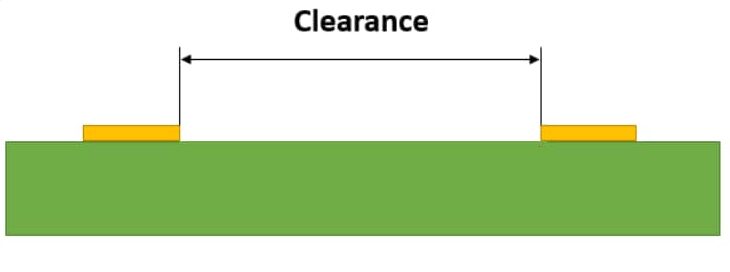
- Distance Between Trace and Reference Plane: The distance between a signal trace and its adjacent reference plane (ground or power plane) is inversely proportional to impedance. Closer spacing reduces impedance, while greater spacing increases it. Proper spacing is critical for maintaining controlled impedance and preventing crosstalk in high-speed circuits.
- Copper Trace Thickness and Roughness: Copper foil thickness has an inverse relationship with impedance—thicker copper results in lower impedance. Designers can control copper thickness by using pattern electroplating or selecting base materials with the appropriate foil thickness. Additionally, copper surface roughness can affect signal loss, particularly at high frequencies, due to the skin effect.
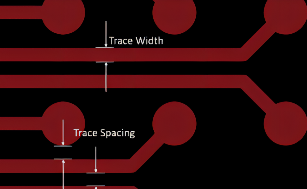
- Trace Width: Trace width is inversely proportional to impedance—wider traces have lower impedance, while narrower traces have higher impedance. To ensure effective impedance control, trace width must be maintained within a tolerance of ±20%. This requires engineering compensation on photomasks to account for etch undercut, lithographic errors, and pattern transfer inconsistencies.
For high-frequency signals, PCB designers must carefully select trace dimensions and layer stackups to achieve the target impedance within the required tolerance. Advanced electronic CAD (ECAD) tools can automatically calculate impedance values based on these parameters, simplifying the design process.
Why is Impedance Matching Required?
The primary function of a PCB trace is to transfer signal power from the driver device to the receiver device. For maximum power transfer to occur, the impedance of the trace must match the impedance of the driver and receiver. This is based on the maximum power transfer theorem, which states that maximum power flows between two devices when their impedances are equal.
A common misconception is that a circuit’s clock speed determines whether it is classified as “high-speed.” In reality, high-speed signals are defined by their rise and fall times—the speed at which a signal transitions between logic 0 and logic 1 states. Even circuits with moderate clock speeds can behave as high-speed circuits if their signal rise/fall times are fast enough, making impedance matching critical.
How to Calculate PCB Trace Impedance?
Calculating PCB trace impedance accurately is challenging due to the many interrelated factors involved. While some open-source tools can provide rough estimates, they often lack the precision required for high-frequency designs. The most reliable approach is to work with your PCB manufacturer, who can use calibrated impedance calculation tools tailored to their specific manufacturing processes.
Key Features of a Reliable Impedance Calculator
- Trace Type Selection: Support for common transmission line types, including microstrip, stripline, differential pairs, and coplanar waveguides.
- Parameter Input: Ability to enter critical parameters such as trace width, trace thickness, dielectric constant, dielectric thickness, and distance to the reference plane.
- Real-Time Calculations: Instant display of characteristic impedance values based on input parameters, allowing for quick adjustments during design.
- Material Database: Preloaded properties for common PCB materials (e.g., FR4, Rogers) to ensure accurate calculations aligned with real-world manufacturing.
To use these tools, simply select the transmission line type, input the relevant parameters, and the calculator will generate the characteristic impedance. This ensures that your design meets the required specifications, particularly for high-speed and RF applications. GET A FREE DESIGN CONSULTATION
What Calculations Does Impedance Control Involve?
As trace length or signal frequency increases, the need for precise impedance adaptation grows. Even minor oversights during the design phase can increase circuit switching times and lead to unexpected errors. Once components are mounted, uncontrolled impedance becomes extremely difficult to analyze, as component tolerances can vary between batches.
Impedance control methods involve calculating the critical length of traces based on signal speed. This critical length is the point at which transmission line effects become significant, making impedance matching essential. Designers must collaborate closely with manufacturers early in the design process to ensure that component values and trace characteristics comply with impedance requirements.
Methods to Achieve Impedance Matching
Controlled impedance means that the trace impedance remains constant at every point along its path, from the signal source to the destination—even when the trace changes layers. Achieving this requires careful attention to design details and adherence to best practices. Many signal reflection and EMI issues can be prevented through proper PCB design techniques, including the following:
1. Use Materials with Low Dielectric Constant
Traditionally, FR4 has been the standard substrate for PCBs. However, for high-speed designs, selecting the right laminate is critical. Materials with a lower dielectric constant (Dk) are preferred, as they minimize signal distortion, phase jitter, and propagation delay. Designers should select a substrate that aligns with their application requirements and specify it clearly in their manufacturing notes.
2. Ensure Proper Signal Return Paths
Including power or ground planes as signal return paths directly below each signal trace is essential for impedance control. Avoiding discontinuities in these planes—such as splits or gaps under critical routing—ensures that return path currents follow the same physical path as the signal, minimizing impedance variations and crosstalk.
3. Optimize Layer Stackup
Layer stackup refers to the arrangement of signal layers, ground planes, power planes, and dielectric materials in a PCB. A well-designed stackup is critical for impedance control, as it stabilizes the impedance of signal traces. Signal layers should be placed adjacent to reference planes (ground or power) to maintain consistent impedance. Controlled impedance traces, such as microstrip and stripline, are designed by adjusting trace width, layer placement, and dielectric properties to meet target impedance values.
Additional design considerations include:
- Keeping trace lengths as short as possible to minimize transmission line effects.
- Selecting the appropriate number and placement of decoupling capacitors to stabilize the power distribution network.
- Avoiding routing stubs and discontinuities, which degrade signal quality.
- Ensuring equal length for differential pair traces to maintain signal synchronization.
- Minimizing inductance from poor component packaging.
- Using immersion silver as a surface finish instead of ENIG, as nickel in ENIG contributes to signal loss at high frequencies due to the skin effect.
Impedance Control Verification
After PCB manufacturing, impedance control can be verified using test coupons—small PCB sections fabricated on the same panel as the main PCBs, typically at the edges. Test coupons replicate the trace dimensions, layer stackup, and material properties of the main PCB, ensuring accurate impedance testing.
A Time-Domain Reflectometer (TDR) is used to measure impedance. The TDR sends a high-speed electrical pulse down the test coupon trace; any impedance discontinuities cause part of the pulse to reflect back. By analyzing the reflected signal, engineers can calculate the characteristic impedance of the trace. A detailed report is then generated to confirm whether the impedance meets the specified requirements. For high-frequency applications above 5 GHz, some manufacturers use Vector Network Analyzers (VNA) to measure S-parameters and convert them to impedance values for greater accuracy.
The overall performance and EMC (Electromagnetic Compatibility) of electronic equipment depend not only on circuit design and layout geometry but also on the power distribution network. Proper impedance control ensures that both signal integrity and power integrity are maintained.
Conclusion
The actual impedance experienced in a PCB layout often differs from the ideal values calculated during the schematic design phase. This discrepancy is primarily due to the presence of the substrate and the physical layout of traces, leading to issues such as crosstalk, ringing, and power integrity problems—especially at high frequencies. As signal speeds continue to increase, the impedance of the power delivery network can deviate from optimal capacitive behavior, further impacting signal and power integrity.
By understanding the factors that cause impedance mismatch and implementing best practices for impedance control, PCB designers can create robust, manufacturable designs that deliver reliable performance. Collaborating with manufacturers early in the design process ensures that impedance requirements are met, reducing prototype iterations and ensuring that the final PCB performs as intended in high-speed and high-frequency applications.
GET A FREE DESIGN CONSULTATION
About US
Founded in 2012, JKRGLO strives to build a one-stop platform for the electronic industry chain. By integrating PCB manufacturing, component procurement and PCB assembly services, we enable digital PCBA processing. With increasing investment in innovation and digital systems, we have achieved rapid growth and emerged as a leading PCB and PCBA manufacturer in the industry, capable of rapidly producing high-reliability and cost-effective products.