
Key Design Principles for Reliable Flex PCBs
Flexible Printed Circuit Boards (Flex PCBs) have become indispensable in modern electronic design, enabling sleek, compact, and lightweight devices that rigid PCBs simply cannot accommodate. From smartphones and wearables to automotive electronics and medical devices, Flex PCBs facilitate seamless wiring, component fitting, and power delivery in space-constrained applications.
Unlike rigid PCBs, which excel in supporting heavy components like CPUs and GPUs, Flex PCBs are engineered to bend, fold, and conform to complex shapes—making them ideal for portable and miniaturized electronics. However, their unique flexibility and material properties demand specialized design and fabrication practices to ensure performance, durability, and manufacturability. Drawing on industry expertise and practical fabrication insights, here are essential design principles to master Flex PCB development.
1. Maintain Proper Bend Radius Specifications
The bend radius is the most critical parameter in Flex PCB design, as improper bending is responsible for over 70% of flex circuit failures. Failing to adhere to minimum bend radius requirements leads to copper fatigue, trace cracking, and layer delamination, especially after repeated bending cycles. IPC-2223 standards define clear guidelines based on the number of layers and bending type:
- For single-layer Flex PCBs: Use a minimum static bend radius of 6x the total board thickness and a dynamic bend radius (for repeated flexing) of 20–25x the total thickness.
- For double-layer Flex PCBs: Maintain a static bend radius of 12x the total thickness and a dynamic bend radius of 40–50x the total thickness.

Avoid sharp bends and ensure bend areas are free of components, vias, and heavy copper traces to distribute mechanical stress evenly.
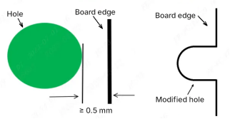
2. Choose the Right Coverlay Instead of Solder Mask for Flex Zones
On Flex PCBs, coverlay serves as the primary protective layer, replacing the solder mask used in rigid PCBs. Coverlay is a polyimide film with adhesive that bends with the circuit, providing superior insulation, abrasion resistance, and mechanical support compared to liquid solder mask. Unlike solder mask, which is prone to cracking under repeated bending, coverlay maintains integrity in dynamic flex zones.
Key design considerations for coverlay include: Pre-windowing the coverlay before lamination to ensure precise pad openings; maintaining a 0.2mm gap between pads and adjacent traces; and using bridged apertures for tight spacing (<0.5mm) to expose connecting traces without compromising protection. For rigid-flex boards, solder mask can be used on rigid sections, but coverlay is mandatory for flexing areas.
3. Incorporate Stiffeners for Critical Areas
Flex PCBs are inherently flexible, but certain areas—such as component mounting sites, connector interfaces, and assembly handling points—require rigidity to prevent deformation. Stiffeners (rigid reinforcement plates) provide localized rigidity while preserving flexibility in other sections, reducing issues like component lifting during reflow soldering and connector contact failure.
Select stiffener materials based on your design needs:
- Polyimide (PI): Ideal for thin profiles and ZIF connector interfaces, matching the Flex PCB’s thermal expansion coefficient (CTE) for better compatibility.
- FR-4: Cost-effective for SMT component mounting areas, offering high rigidity per unit cost.
- Stainless Steel: Suitable for space-constrained designs requiring maximum rigidity and EMI shielding.
Ensure stiffeners are bonded securely to the Flex PCB and aligned with component footprints to avoid assembly issues.
4. Optimize Trace Routing for Flexibility and Signal Integrity
Trace routing on Flex PCBs requires a balance between flexibility and signal performance. Avoid right-angle bends, which create stress concentration points that can crack during bending. Use 45-degree angles or rounded corners instead to distribute stress evenly. Keep trace widths consistent—sudden changes in width can cause signal reflections and mechanical weakness.
For high-speed signals, route traces parallel to the direction of bending to minimize signal loss and crosstalk. Maintain uniform spacing between traces (at least 0.15mm) to prevent short circuits and ensure signal integrity. Avoid routing traces over bend lines whenever possible; if unavoidable, use wider traces to enhance durability.
5. Prevent Copper Delamination and Oxidation
Copper layers on Flex PCBs are prone to delamination and oxidation, especially in high-temperature or humid environments. To mitigate this, avoid large solid copper areas, as they can trap air during coverlay lamination—leading to oxidation under heat and pressure.
Practical solutions include: Using hatched (grid) copper patterns to reduce surface area and allow air venting; adding solder mask windows in non-flexing areas to release trapped air; and selecting appropriate surface finishes (such as ENIG or OSP) to protect copper from oxidation. Ensure proper lamination pressure and temperature to bond copper layers securely to the polyimide substrate.

6. Design Connector Pads for Durability and Easy Assembly
Connector pads are critical to Flex PCB performance, as they facilitate reliable electrical connections and easy replacement during repair. Use solder mask-defined (SMD) pads for connectors to enhance mechanical strength, as the solder mask coverage on the pad’s rim provides additional support.
Key recommendations: Ensure coverlay overlaps connector pads by at least 0.3mm to prevent pad lifting; shrink gold finger lengths by 0.2mm to avoid micro-shorts from laser cutting; and offset pads on opposite sides of the Flex PCB to improve adhesion. For ZIF connectors, use stiffeners beneath the pad area to maintain flatness and ensure secure mating.
Conclusion
Designing reliable Flex PCBs requires a deep understanding of their unique mechanical and thermal properties, as well as adherence to specialized design principles. By following these six essential guidelines—maintaining proper bend radii, using coverlay correctly, incorporating stiffeners, optimizing trace routing, preventing copper oxidation, and designing durable connector pads—engineers can significantly improve the durability, manufacturability, and performance of their flex circuit designs.
Flex PCBs continue to evolve, with growing applications in emerging technologies like foldable electronics and automotive ADAS systems. This guide serves as a foundational resource for engineers new to Flex PCB design, while also offering practical insights for experienced designers looking to optimize their layouts. Stay tuned for more in-depth guides on Flex PCB materials, fabrication techniques, and advanced design strategies on our blog.
About US
Founded in 2012, JKRGLO strives to build a one-stop platform for the electronic industry chain. By integrating PCB manufacturing, component procurement and PCB assembly services, we enable digital PCBA processing. With increasing investment in innovation and digital systems, we have achieved rapid growth and emerged as a leading PCB and PCBA manufacturer in the industry, capable of rapidly producing high-reliability and cost-effective products.