
Stop Wasting Thousands On Field Failures: The 7 PCB Testing Methods You Actually Need
Bare Board Test: The Pre-Assembly Check That Stops 30% Of Headaches Before You Solder A Single Part
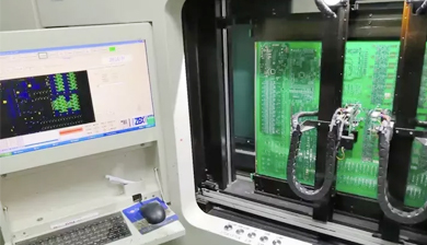
Flying Probe Test: The Prototype Hero That High-Volume Shops Refuse To Touch
Flying probe test uses two or more moving probes to test electrical points on a populated board, no custom fixture required. It’s perfect for prototypes and low-volume runs, because you can set it up in hours for a new design, with zero upfront fixture cost. The catch? It’s slow. For a 1000-unit run, it will take days longer than ICT. For high-volume production, it’s not feasible. For prototyping, design validation, and low-volume high-mix work? It’s non-negotiable.
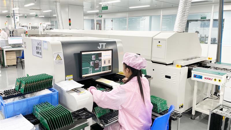
In-Circuit Test (ICT): The High-Volume Workhorse With A Hidden Upfront Cost
ICT is the gold standard for high-volume, stable designs. It uses a custom bed-of-nails fixture to test hundreds of points on a board in seconds, catching component value errors, shorted or open circuits, and dead components with near 98% accuracy. The catch? That custom fixture can cost $3,000 to $10,000, and it only works for that exact board design. If you’re tweaking your design every few months, or running small batches, that upfront cost will eat your margins alive. If you’re running 10,000+ units of a locked design? It pays for itself in the first batch.

AOI: The AI-Powered Upgrade That’s Killing Manual Inspection In 2026
Automated Optical Inspection uses high-resolution cameras to scan your board pre- and post-solder, catching missing components, incorrect parts, solder bridges, and component offset. 2026 industry data shows that AI-integrated AOI systems now make up 67% of new AOI installations, up from 38% in 2024. These systems cut false failure rates by 72% compared to legacy AOI tools, and can catch fine-pitch component defects down to 5μm — critical for the HDI boards powering 6G and automotive ADAS systems that are dominating new design wins this year. Manual inspection can’t match this speed, accuracy, or consistency, and most shops are phasing it out entirely for production runs.
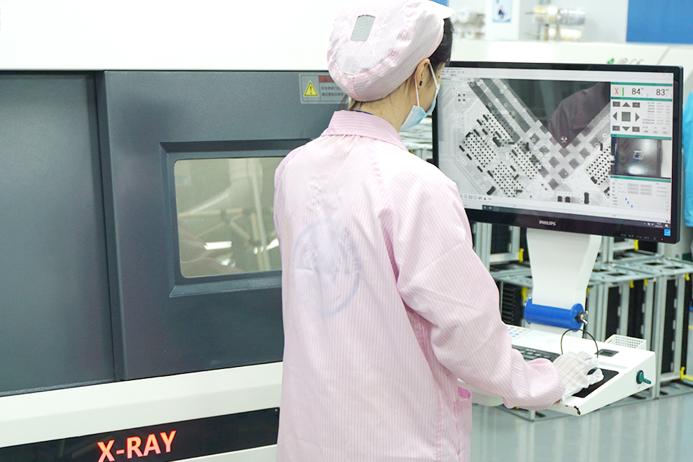
X-Ray Inspection: What Your Eyes (And AOI) Can’t See, This Will Catch
AOI can only see what’s on the surface of your board. X-ray inspection sees everything. It’s the only way to validate hidden solder joints on BGA and CSP packages, buried vias, and inner layer connections on multi-layer HDI boards. We’re also seeing a 42% year-over-year rise in X-ray inspection adoption for high-reliability boards in 2026, as ISO 26262 and IATF 16949 requirements push more manufacturers to switch from sampling to 100% inspection of these hidden features. If your board uses BGA packages or has buried vias, this isn’t optional.
Boundary Scan Test: For Complex Boards Where Probes Can’t Reach
For boards with dense BGA packages, multi-layer HDI designs, or components packed so tight there’s no room for test points, boundary scan (also known as JTAG testing) lets you validate the connectivity between integrated circuits without physical probe access. It uses the test access port built into most modern ICs to check pin-level connections and inter-IC communication, without needing to probe every individual point. It’s not for simple 2-layer boards. For complex digital boards with limited physical access? It’s the only way to get full test coverage.
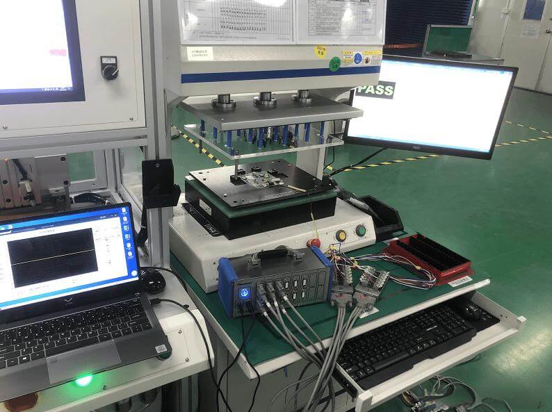
Functional Circuit Test (FCT): The Final Gate That Separates Good Boards From Field Failures
FCT is the final test before your board ships. It runs your board through its full operating cycle, under the same voltage, load, and environmental conditions it will see in the end application. It validates that the board does exactly what it’s designed to do, not just that its individual components work. It won’t catch every tiny upstream defect, but it will catch the ones that will make your board fail when it’s in the hands of your customer. This is the one test that no production run should skip, no matter the volume.
Now that we’ve broken down each method, here’s a side-by-side look at how they stack up, for anyone still asking What are the 7 types of PCB testing methods? and needing a quick, actionable reference.
| Test Type | Best For | Cost Per Run | Speed | Core Defects Caught | Ideal Production Volume |
|---|---|---|---|---|---|
| Bare Board Test | Unpopulated PCBs | Low | Fast | Shorted/Open Traces, Drill Misalignment, Impedance Mismatch | All Volumes (Mandatory Pre-Assembly for High-Reliability) |
| Flying Probe Test | Prototypes, Low-Volume Runs | Low-Medium | Slow | Component Placement, Solder Joints, Electrical Continuity | Prototyping, Low-Volume (<1,000 Units) |
| In-Circuit Test (ICT) | High-Volume, Stable Designs | High (Upfront Fixture Cost) | Very Fast | Component Values, Shorted/Open Circuits, Dead Components | High-Volume (>10,000 Units) |
| Automated Optical Inspection (AOI) | Pre/Post-Solder Assembly | Medium | Fast | Solder Defects, Component Offset, Missing/Incorrect Parts | All Volumes |
| X-Ray Inspection | BGA/CSP Packages, Buried Vias, HDI Boards | High | Medium | Hidden Solder Joint Defects, Voiding, Inner Layer Misalignment | High-Reliability, Complex HDI Designs |
| Boundary Scan Test | Complex Multi-IC Boards, Limited Probe Access | Medium | Medium | Inter-IC Connectivity, Pin-Level Defects | High-Density, Complex Digital Boards |
| Functional Circuit Test (FCT) | Final End-Use Validation | Medium-High | Medium | Full System Performance, Load Testing, Environmental Compatibility | All Volumes (Final Gate) |
Production Floor Truth: You Don’t Need All 7 Tests
Real Questions From Real Engineers (No Fluff Answers)
Let’s be blunt. This is the single most common mistake I see new manufacturers make. FCT will tell you if your board works at the end of the line. It won’t tell you why it doesn’t work. It won’t catch a cold solder joint that will fail after 100 hours in the field. It won’t catch a 5% impedance mismatch that will tank your RF performance in extreme temperatures. I’ve seen clients try this shortcut, and 9 times out of 10, they end up with a pile of non-functional boards that they can’t troubleshoot, and a bill that’s 10x what they saved by skipping earlier tests. FCT is the final gate, not a replacement for targeted upstream checks.
Which test gives me the best ROI for low-volume, high-mix production?
Flying probe test paired with AI-integrated AOI. Full stop. Here’s why: ICT requires a custom fixture that can cost $3,000-$10,000 per design, which makes zero sense if you’re only running 50-500 units per board. Flying probe has no fixture cost, can be set up in hours for a new design, and catches all the critical electrical defects. Pair it with modern AOI to catch solder and placement issues that probes might miss, and you’ve got a test flow that costs a fraction of full ICT, while catching 95% of the defects that will sink your batch. For high-mix, low-volume work, this is the only combination that makes financial sense, without sacrificing reliability.
At the end of the day, the right test mix isn’t about checking every box on a textbook list. It’s about picking the methods that fit your design, your volume, and your tolerance for risk. I’ve spent 10 years on production floors, fixing test flows that were either wasting thousands on unnecessary steps, or missing critical defects that cost clients their biggest contracts.