
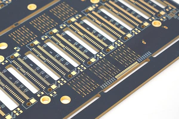
High Frequency PCB
HOME / High Frequency PCB
What is a High Frequency PCB?
As the frequency increases beyond a certain limit, signal losses in standard FR4 boards rise significantly. To address this, we offer a range of High-Frequency PCBs, designed specifically for MHz to GHz applications. These boards use low-loss dielectric materials with a reduced loss tangent, minimizing signal degradation. This ensures controlled electromagnetic interference (EMI) and reliable, high-speed signal transmission.
Common Materials for High Frequency PCB
Unlike standard FR4 boards, High-Frequency PCBs can be selected based on Dk (dielectric constant) and Df (dissipation factor). The lower these values, the better the signal integrity at high frequencies. Some materials JLCPCB offers include:
Rogers Material:
RO4350B (Dk=3.48, Df=0.0037)
Rogers-RO4350B:
This material is a strengthened glass hydrocarbon/ceramic material with a dielectric constant of 3.48 at 10GHz, which makes it commonly used in high-frequency power amplifier designs. The RO4350B laminate has a low Z-axis coefficient of thermal expansion (CTE), which ensures high stability of multilayer circuits interconnected by plated through holes (PTH).
PTFE Teflon Material:
ZYF255DA (Dk=2.55, Df=0.0018)
ZYF265D (Dk=2.65, Df=0.0019)
ZYF300CA-C (Dk=2.94, Df=0.0016)
ZYF300CA-P (Dk=3.0, Df=0.0018)
Rogers-RO4350B:
PTFE Teflon PCB has outstanding comprehensive performance in practical use and is an ideal material choice for high-complexity and high-reliability designs. It has good temperature resistance, strong heat dissipation, excellent dielectric properties, and good mechanical stability. It is very durable in use and can withstand a certain amount of oxidation and UV rays, so it is also a cost-effective option.
The Benefits of JKRGLO High Frequency PCB
Low Dielectric Loss
Lower loss in PCB dielectric means higher signal strength. Dielectric losses can cause EMI failure and excessive crosstalk. With a low dissipation factor (Df), signal losses can be controlled at high frequencies.
Stable Performance at High Speeds
At high speed, signals travel in dielectric space, and copper traces act as waveguides. Substrate having lower loss tangent (Df) ensures better signal performance throughout.
Excellent Signal Integrity
Factors like impedance mismatch and signal delays increase if the substrate has higher parasitic components. With high-frequency substrates, delays can be controlled in RF and high-speed circuits.
High Frequency PCB Design Considerations
1. Controlled Impedance
Trace width, spacing, and dielectric properties are used to tune the impedance. Impedance matching should be there for better signal transmission. That’s why in RF transmission lines 50Ω, 75Ω, and 100Ω are used.
2. Material Thermal Expansion Coefficient
Copper traces are placed on top of the substrate to form the electrical circuit. As the temperature changes, the substrate expands, and so does the copper. If there is a large mismatch, the traces can be damaged or broken.
3. Copper Foil Type and Plating
A good copper foil with a smooth surface and low resistance ensures lower losses at microwave frequencies. Plating choices such as ENIG or immersion silver must balance conductivity and reliability.
Common Applications of High Frequency PCBs
1. RF and Microwave Systems
RF and microwave systems operate in the 3 kHz to 300 GHz range, and high-frequency applications often require specialized materials. Materials like Rogers are therefore used to design RF front-end modules that demand high accuracy and minimal signal distortion.
2. 5G Infrastructure
Communication nowadays works with weak, small signals, and they need to be detected with a higher probability for reliability. These materials are used where ultra-low latency and high bandwidth are required.
3. Satellite Communication
Satellites are objects we send to space, and with a lot of investment, we do not want system failures due to external radiation and EMI. So these materials are used to handle long-range and high-frequency signals.
JKRGLO High Frequency PCB Manufacturing Capabilities
High Frequency PCB Manufacturing Capabilities
| Features | Capabilities |
|---|---|
| Minimum Drill | 0.2mm |
| Minimnum Track Width and Spacing | 0.10 / 0.10 mm (4 / 4 mil) |
| Minimum Dimensions | 3 × 3mm |
| Maximum Dimensions | 590*438mm |
| Layer | 2-layer |
| Thickness | 0.65mm,0.9mm,1.65mm |
| Copper Weight | 1oz |
| Soldermask Color | Green |
| Silkscreen | White |
| Surface finish | ENIG |
| Gold Thickness | 1U", 2U" |
Why Choose JKRGLO as Your High Frequency Manufacturer?
High-Frequency Performance
JKRGLO offers High Frequency PCBs using advanced materials like Rogers RO4350B and PTFE Teflon, delivering low-loss performance with a Dk of 2.55-3.48 and Df as low as 0.0016. These materials ensure exceptional signal integrity for high-speed applications from 1GHz to 40GHz.
Reliable Quality Assurance
JKRGLO’s industry-leading quality assurance process guarantees that each PCB undergoes rigorous testing, ensuring reliable and consistent performance at high frequencies. JKRGLO maintains high standards, so you can trust your designs to perform under demanding conditions.
Competitive Pricing
JKRGLO provides cost-effective solutions without compromising performance, making cutting-edge technology more accessible to your budget.
Fast Prototyping
With a 4-5 day prototyping turnaround, JKRGLO ensures fast delivery without sacrificing quality, so you can iterate and refine designs quickly.
Submit a High Frequency PCB Quote Now
Frequently Asked Questions About High Frequency PCB
What frequency range do high-frequency PCBs cover?
Typically, frequencies above 500MHz to a few GHz are used for RF, microwave, and 5G applications.
Why is Rogers material preferred over FR4 for high-frequency PCBs?
Rogers has lower dielectric loss and a more consistent dielectric constant. Dk and Df are relatively low, which is best for high-speed designs.
Can high-frequency PCBs be multi-layered?
Multi-layer stack-ups are common for complex RF and 5G designs requiring power/signal separation.
What are the challenges in manufacturing HF PCBs?
Precise impedance control, thermal management, and material handling are critical challenges compared to standard PCBs.