What is GND in a Circuit? Ground Types, Common Return Paths, and PCB Layout Rules
서론
The Four Types of GND Symbols in Schematics
| Ground Type | Schematic Symbol | Physical Connection | Primary Application |
|---|---|---|---|
| Earth Ground (GND_E) | Triangle pointing down to a vertical line | Physical connection to the Earth via a grounded stake or mains pin | Heavy machinery, AC mains power supply safety, lightning protection |
| Chassis Ground (GND_C) | Diagonal lines (hatching) tied to a frame | Metal enclosure or mechanical casing of the product | ESD shielding, safety grounding, EMI containment |
| Analog Ground (AGND) | Triangle labeled 'A' or clean ground return | Isolated low-noise copper return path | Precision ADCs, operational amplifiers, sensor front-ends |
| Digital Ground (DGND) | Solid shaded triangle or 'D' label | High-speed switching return plane | Microcontrollers, FPGA logic, high-speed buses |
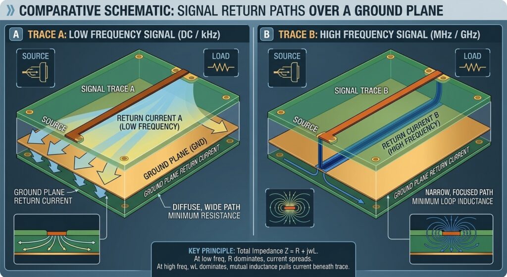
High-Frequency Return Current: The Rule of Minimum Inductance
A common misconception among junior layout engineers is that return current takes the path of minimum resistance. While true for Direct Current (DC), alternating current (AC) and high-speed digital signals behave differently.
Return current always follows the path of minimum impedance (Z), where:
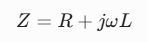
At frequencies above 100kHz, the inductive reactance term (jωL) dominates the resistive term (R). Consequently, return current pulls itself directly underneath the signal trace on the adjacent reference plane to minimize loop area (A) and loop inductance (L).

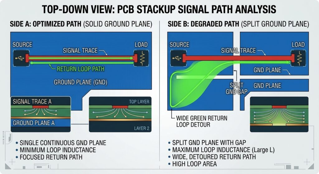
If a slot, split plane, or cutout intersects this return path, the return current must detour around the obstruction. This creates a large inductive loop area, causing:
Ground Bounce: Local voltage spikes across the ground plane.
EMI Radiation: The slot acts as an unintended slot antenna radiating electromagnetic noise.
Crosstalk: Overlapping return paths coupling noise into adjacent traces.
5 Essential PCB Grounding Rules of Thumb
To comply with IPC-2221 layout guidelines and pass EMC testing (such as FCC Part 15 or CE Class B), follow these layout constraints:
Maintain an Unbroken Solid Reference Plane: Avoid routing signal traces across split ground planes. If a trace must change layers, place a stitching via immediately adjacent to the signal via to allow the return current to transition smoothly between reference layers.
Single-Point Net Ties for AGND and DGND: Never tie Analog Ground and Digital Ground together randomly across the board. Connect them at a single point—typically at the Analog-to-Digital Converter (ADC) chip or via a zero-ohm resistor / ferrite bead—to prevent noisy digital switching currents from corrupting sensitive analog readings.
Keep ESD Return Paths Short: Connect TVS (Transient Voltage Suppressor) diodes and chassis ground mounts with wide, low-inductance traces directly to the main system ground to safely shunt electrostatic discharge away from core ICs.
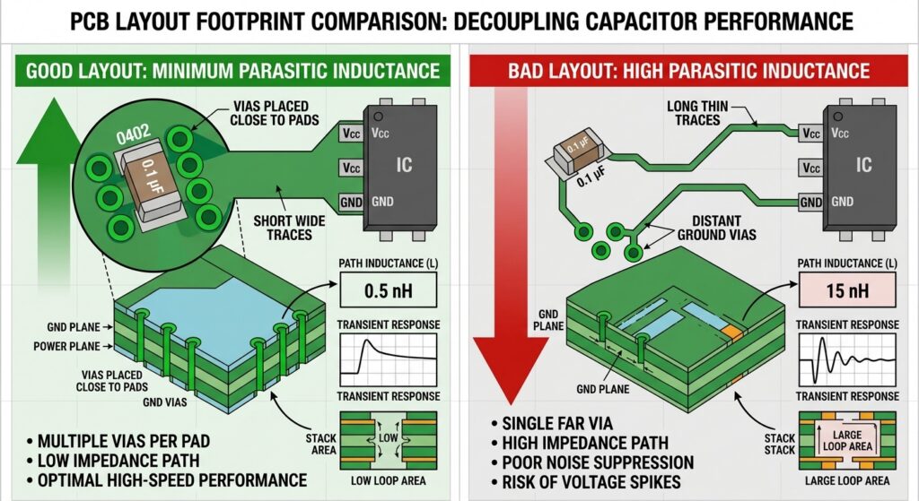
Decoupling Capacitor Placement: Place decoupling capacitors (e.g., $100\text{nF}$ MLCCs) as close as physically possible to the IC power pins. Connect the capacitor’s ground pad directly to the inner ground plane using a dedicated, short via to minimize parasitic loop inductance.
Implement Star Grounding for Power Supplies: In SMPS (Switch-Mode Power Supply) layouts, run high-current power return paths back to the output capacitor in a star topology rather than tying them into sensitive control signal grounds.
Ground Layout Reference Summary
| Design Challenge | Cause | Grounding Solution |
|---|---|---|
| Ground Bounce | High $di/dt$ switching through via/trace inductance | Use wide solid ground planes; place decoupling capacitors close to IC power pins |
| Radiated EMI / Failed EMC | Large return current loop area caused by plane slots | Eliminate splits beneath high-speed signals; add ground stitching vias near signal layer transitions |
| ADC Noise / Jitter | Digital ground noise coupling into analog ground | Use star grounding or a single-point net tie underneath the converter IC |
| ESD Damage | High-voltage transients entering signal paths | Route TVS diode ground pins directly to chassis/earth ground with short, wide traces |
자주 묻는 질문 (FAQ)
What is the difference between Neutral and Ground?
In AC power systems, Neutral is a current-carrying conductor that completes the circuit back to the power source under normal operation. Ground (Earth Ground) is a safety conductor designed to carry current only during a fault condition (such as a short circuit to a metal enclosure) to trip circuit breakers and prevent electric shock.
Can a circuit function without an Earth Ground connection?
Yes. Battery-powered devices (such as smartphones or laptops) operate on a floating ground (local signal reference plane) without any physical connection to the Earth. Ground in these systems simply serves as the common zero-volt reference for onboard electronics.
Is a single continuous ground plane better than split AGND/DGND planes?
For most modern mixed-signal PCBs, a single, continuous ground plane is superior to physically split planes, provided components are grouped effectively into distinct analog and digital zones. Physical splits often create accidental return-path slots when traces cross the gap, causing severe EMI issues.
회사 소개

저자 소개
앤드류 잔 – JKRGLO.com 연구개발(R&D) 엔지니어
앤드류 잔(Andrew Zhan)은 PCB 업계에서 14년 이상의 연구개발(R&D) 엔지니어링 경력을 쌓아왔으며, 회로 설계 최적화 및 DFM 구현 분야에서 깊은 전문성을 보유하고 있습니다. 그는 복잡한 설계 요구 사항을 양산 가능한 솔루션으로 전환하는 데 주력하며, 시제품 제작과 양산 모두에서 기술 혁신을 주도하고 있습니다.
그는 여러 부서의 팀 및 고객과 긴밀히 협력하며, 프로젝트의 전체 수명 주기 동안 철저한 품질 검증과 원활한 기술적 소통을 보장합니다. 앤드류는 고객의 기대를 꾸준히 뛰어넘는, 신뢰할 수 있고 고성능의 PCB 솔루션을 제공하는 데 전념하고 있습니다.
목차
그래도 도움이 필요하신가요? 문의하기:
PCB 또는 PCBA 견적이 필요하신가요?
태그:
pcb order
gnd definition