
Flexibility Combined with Strength: A Comprehensive Guide to Rigid-Flex PCB Technology
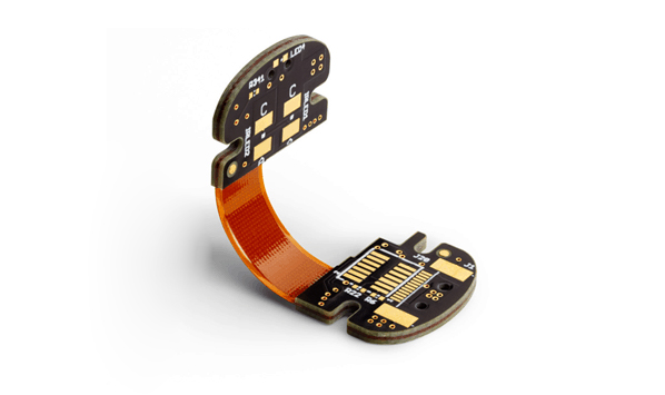
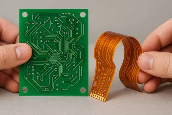
In the fast-paced world of electronics, the pursuit of smaller, more reliable, and versatile devices has become a driving force for technological innovation. To keep pace with these evolving demands, engineers and designers are increasingly adopting Rigid-Flex PCBs—circuit boards that seamlessly integrate rigid and flexible substrates into a single interconnected structure. This unique combination enables complex designs that can bend and flex in specific areas while maintaining structural rigidity in others, striking the perfect balance between adaptability and stability. Technically, Rigid-Flex PCBs consist of two or more conductive layers separated by either flexible or rigid insulation materials, with industry standards like IPC providing guidelines for optimal design and manufacturing.
The rigid sections of these boards serve as the backbone, housing electronic components and providing essential structural support, while the flexible sections allow for bending, folding, and twisting, enabling more compact and intricate device designs. Most Rigid-Flex PCBs are constructed with multiple layers of flexible circuit substrates attached to one or more rigid boards—either externally, internally, or both—depending on the specific requirements of the application. In this guide, we’ll explore the fundamentals of Rigid-Flex PCB technology, its key benefits, critical design considerations, common applications, and the challenges associated with its design and manufacturing.
Rigid-Flex PCB Design: Beyond Traditional 2D Layouts
Unlike traditional rigid PCBs, which are limited to 2D designs, Rigid-Flex PCBs are designed in three dimensions. This 3D flexibility allows the board to be folded or twisted into custom shapes, maximizing spatial efficiency and making them ideal for compact, weight-sensitive applications such as medical devices, wearable technology, and aerospace equipment. Additionally, Rigid-Flex PCBs are typically thinner than standard rigid boards, thanks to thin copper layers and adhesive-less laminates, making them the perfect solution for products requiring slim, lightweight packaging.
Further Read:How durable are flex boards?
The Evolution of Rigid-Flex PCB Technology
PCB technology has undergone significant advancements over the years, addressing the limitations of earlier designs. Rigid PCBs were once the industry standard, but their inability to bend made them prone to breakage and unsuitable for compact or irregularly shaped devices. Flexible PCBs, while bendable, lacked the structural support needed to house heavy components. Rigid-Flex PCBs emerged as a solution, combining the best of both worlds: the durability and structural stability of rigid PCBs with the flexibility of flexible PCBs.
Originally developed for spacecraft and aerospace applications—where reliability and compactness are critical—Rigid-Flex PCBs have now become ubiquitous in consumer electronics, including smartphones, laptops, and tablets. The flexible sections are typically made from Polyimide (PI), a material known for its high heat resistance and flexibility, while the rigid sections use FR4, a durable and cost-effective epoxy resin composite. Common Rigid-Flex PCB designs include 4-layer, 6-layer, and 8-layer configurations, depending on the complexity of the application.
Rigid-Flex PCB Types: Static vs. Dynamic Applications
Rigid-Flex PCBs are categorized based on their functional applications, with two main types: static (flex-to-install) and dynamic (continuous flexing). The design and construction of the board vary significantly depending on which type of application it is intended for.
Static Application (Flex-to-Install): This type of Rigid-Flex PCB is only required to flex during the installation process, allowing it to fit into the device’s housing. Once installed, the flexible sections remain in a fixed position, with no further bending required.
Dynamic Flexing Applications: In these applications, the flexible sections of the board are dynamically flexed during normal device operation. This can range from a few hundred flex cycles to over one million cycles, depending on the product’s lifespan and usage requirements. Examples include devices with moving parts, such as foldable smartphones and robotic arms.
Key Advantages of Rigid-Flex PCBs
Rigid-Flex PCBs offer numerous advantages over traditional rigid or flexible PCBs, making them a preferred choice for a wide range of applications. Here are the most significant benefits:
1. Space and Weight Savings: By integrating rigid and flexible sections into a single board, Rigid-Flex PCBs eliminate the need for connectors, cables, and other interconnection components. This reduces the overall size and weight of the electronic assembly, making it ideal for compact devices like wearables and medical implants.
2. Enhanced Reliability: The removal of connectors and solder joints in the flexible sections reduces potential failure points. This improves the board’s reliability and extends the product’s lifespan, critical for applications like aerospace and medical devices where downtime is unacceptable.
3. 3D Design Capability: Rigid-Flex PCBs can be designed to fit into three-dimensional spaces, allowing for more creative and efficient device layouts. This is particularly valuable in applications where space is at a premium, such as automotive electronics and portable devices.
4. Superior Mechanical Strength: The rigid sections provide the necessary mechanical support for heavy components, while the flexible sections offer resistance to mechanical stress, vibration, and shock. This combination ensures the board can withstand harsh operating conditions.
Design Considerations for Rigid-Flex PCBs
Designing Rigid-Flex PCBs requires careful planning and attention to detail to ensure optimal performance and manufacturability. Here are the key factors to consider:
Material Selection: Choose compatible materials for the rigid and flexible sections. FR4 is ideal for rigid sections due to its durability and cost-effectiveness, while Polyimide (PI) is the preferred material for flexible sections due to its flexibility and heat resistance. Ensure all materials can withstand the device’s operating temperature and environmental conditions.
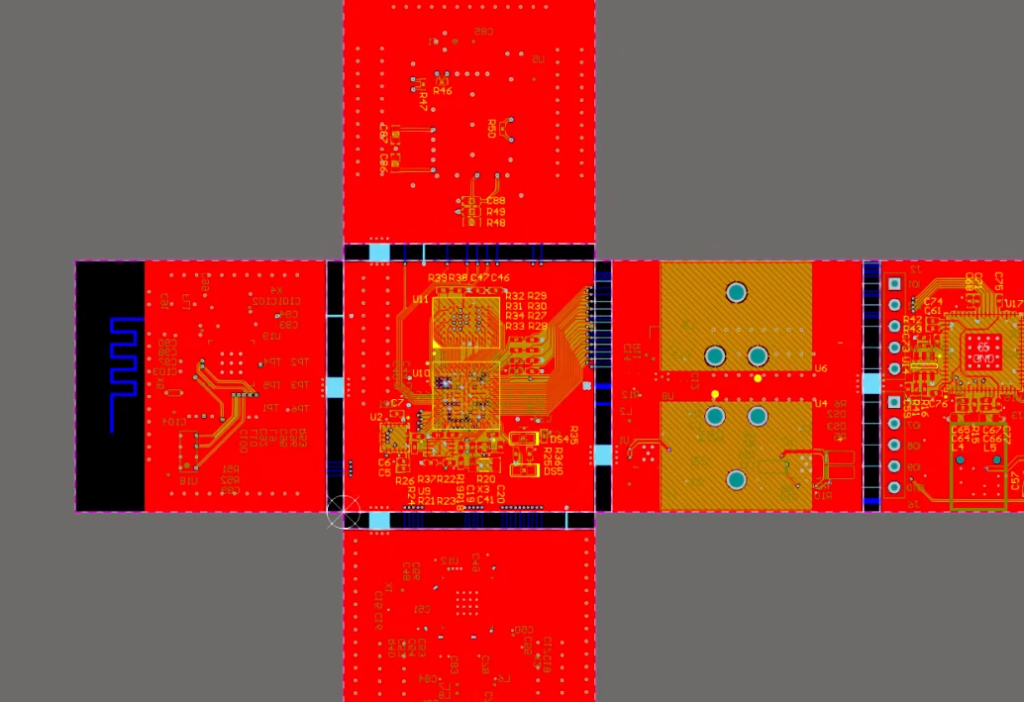
Layer Stack-Up: Design the layer stack-up to balance electrical performance, mechanical strength, and flexibility. The number of layers and the arrangement of rigid and flexible sections will depend on the application’s electrical requirements and bending needs.
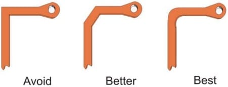
Bending and Flexing: Design the flexible sections with an appropriate bend radius to prevent trace damage. A too-small bend radius can lead to mechanical failure and signal degradation. Implement stress reduction techniques, such as rounded corners and tear drops, to enhance durability.
Component Placement: Position components exclusively on the rigid sections to avoid stress on solder joints during bending. This ensures the components remain secure and functional throughout the device’s lifespan.
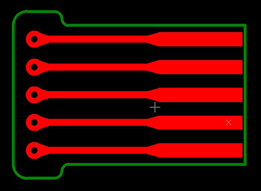
Trace Routing: Plan trace routing to minimize stress during bending. Avoid running traces parallel to the bend axis and ensure traces are wide enough to withstand repeated flexing without breaking.
Impedance Control: For high-speed designs, maintain consistent impedance by carefully controlling trace widths, spacing, and dielectric thickness. This prevents signal reflection and degradation.
Manufacturability: Collaborate with manufacturers early in the design process to address potential complexities. This ensures the design is feasible to produce and reduces the risk of delays or cost overruns.
The Manufacturing Process of Rigid-Flex PCBs
The manufacturing process of Rigid-Flex PCBs is more complex than that of traditional rigid or flexible PCBs, due to the combination of different materials and the need for precise alignment. Here are the key steps involved:
1. Material Preparation: Select and cut the appropriate materials for the rigid (FR4) and flexible (Polyimide) sections.
2. Layer Lamination: Bond the rigid and flexible layers together using adhesive, ensuring proper alignment and bonding strength.
3. Drilling and Plating: Drill holes (vias) to connect different layers, then plate the vias with copper to ensure electrical conductivity between layers.
4. Imaging and Etching: Transfer the circuit pattern onto the board using photolithography, then etch away the unwanted copper to form the conductive traces.
5. Soldermask and Silkscreen: Apply a soldermask to protect the traces from oxidation and short circuits, then add silkscreen annotations for component placement and identification.
6. Final Testing and Inspection: Test the board for electrical performance, continuity, and mechanical durability to ensure it meets the application’s requirements.
Challenges in Rigid-Flex PCB Design
Rigid-Flex PCBs have more complex design rules than traditional rigid PCBs, as they must address both the mechanical and electrical needs of the rigid and flexible sections. Here are the main challenges designers face:
Bend Radius Importance: Selecting the correct bend radius is critical. A radius that is too small can cause the flexible substrate to crack, leading to mechanical failure and signal loss. Designers must consider the material properties and the number of flex cycles when determining the appropriate bend radius.
Tear Drop Design: Adding tear drops to through holes can improve stability and reduce the risk of cracking at the junction of rigid and flexible sections. Tear drops distribute stress evenly, enhancing the board’s durability.
Signal Integrity and EMI: Maintaining signal integrity and controlling electromagnetic interference (EMI) in flexible sections is challenging. The flexible substrate’s properties and the proximity of traces to the bend region can affect signal quality. Designers must use shielding and proper grounding techniques to mitigate these issues.
Round Corner Design: Using rounded corners on the flexible sections prevents corner tearing and improves durability. Sharp corners are prone to stress concentration, which can lead to mechanical failure during bending.
Layer Transition: Properly transitioning signal layers from rigid to flexible sections is critical. Misalignment or improper transitions can cause impedance mismatches, leading to signal degradation and reduced performance.
Conclusion
Rigid-Flex PCBs represent a powerful solution for modern electronic devices that require compact, reliable, and flexible circuit designs. By combining the strengths of rigid and flexible PCBs, they enable innovative design possibilities across a wide range of industries—from consumer electronics to aerospace and medical devices. However, designing and manufacturing Rigid-Flex PCBs requires careful planning, material selection, and collaboration with experienced manufacturers to ensure a successful outcome.
As technology continues to advance, the role of Rigid-Flex PCBs in electronic design will only grow. They will drive innovation in devices that are smaller, lighter, and more reliable, helping engineers stay ahead in the competitive world of electronics. Whether you’re designing a new product or improving an existing one, understanding the intricacies of Rigid-Flex PCB technology is key to unlocking its full potential.
About US
Founded in 2012, JKRGLO strives to build a one-stop platform for the electronic industry chain. By integrating PCB manufacturing, component procurement and PCB assembly services, we enable digital PCBA processing. With increasing investment in innovation and digital systems, we have achieved rapid growth and emerged as a leading PCB and PCBA manufacturer in the industry, capable of rapidly producing high-reliability and cost-effective products.