SMT Quality Inspection Standards: The Acceptance Criteria That Actually Matter
Introduction liminaire
Every PCBA shop claims to “inspect 100%.” What actually separates a good line from a mediocre one is the criteria the inspectors use. If the pass/fail line is vague, bad boards ship. If it’s too strict, good boards get scrapped.
Here are the SMT quality inspection standards we use on our own lines — the same pass/fail thresholds we apply before anything leaves the factory.
Réponse rapide :
What are the SMT quality inspection standards? They’re the measurable acceptance criteria for soldered joints and component placement. The ones that matter most:
- Solder balls are acceptable only if their diameter is ≤0.13 mm.
- Side overhang is acceptable when it stays within 50% of the lead/termination width (or 25% for cylindrical end caps).
- Tombstoning, bridging, and billboarding over 2:1 are rejects, no exceptions.
These numbers come straight from standard IPC-A-610-style acceptance rules, and they’re what a serious PCBA supplier should be able to quote back to you without hesitating.
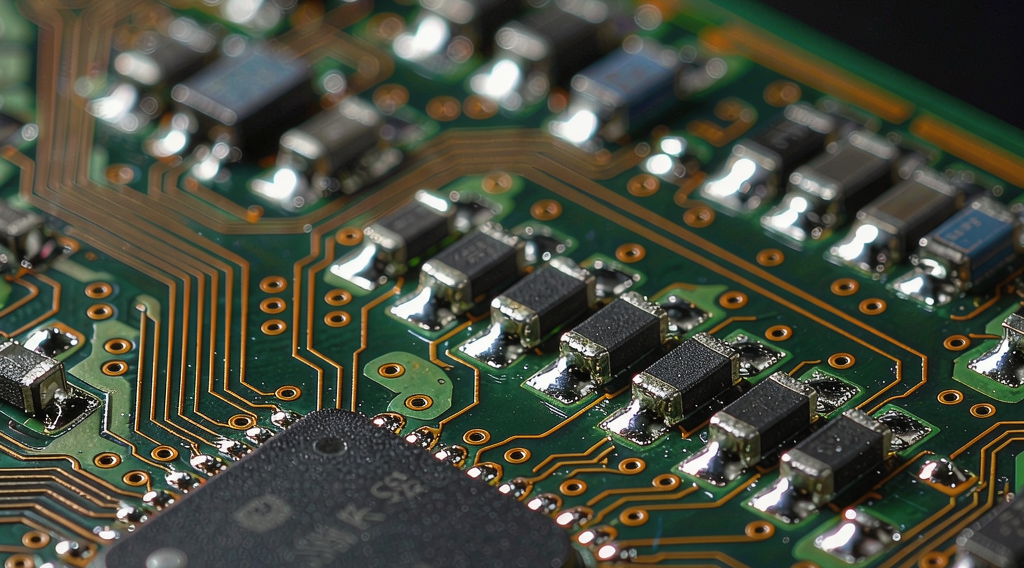
The 8 Acceptance Criteria We Inspect
| # | Defect | Accepter | Reject |
|---|---|---|---|
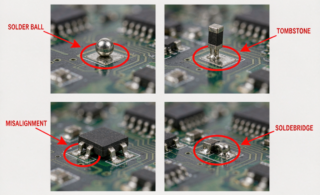
| 1 | Solder ball | Diameter ≤0.13 mm, not trapped in no-clean residue or under conformal coating | Diameter >0.13 mm |
| 2 | Insufficient solder | Solder overlap between termination and pad clearly visible | Solder overlap insufficient |
| 3 | Billboarding | Width-to-height ratio ≤2:1 | Ratio >2:1; termination not fully wetted; parts larger than 1206 |
| 4 | Tombstoning | — | One end of a chip component lifted off the pad |
| 5 | Flat / L / gull-wing lead overhang | Side overhang (A) ≤50% of lead width (W) or 0.5 mm | Overhang >50% of W or 0.5 mm |
| 6 | Cylindrical end-cap overhang | Overhang (A) ≤25% of component width (W) or pad width (P) | Overhang >25% of W or P |
| 7 | Chip (rectangular/square) overhang | Overhang (A) ≤50% of termination width (W) or pad width (P) | Overhang >50% of W or P |
| 8 | J-lead overhang & bridging | Overhang (A) ≤50% of lead width (W); no bridging | Overhang >50% of W; solder bridges between conductors |
Two things worth pointing out. First, “overhang” and “offset” are tolerance windows, not aesthetic preferences — a lead sitting at 40% overhang is fine even if it looks slightly off. Second, the 0.13 mm solder-ball limit and the 25% cylindrical cap rule are the two thresholds novices most often get wrong, because they’re tighter than they look.
Three PCB Design Mistakes That Cause Inspection Failures
Most SMT defects aren’t born on the line — they’re baked into the design. These three come up constantly:
- Unclear layer definition. If a single-sided board is designed on the TOP layer without a note, the fabricator can’t tell which side is front and which is back. The board comes back hard to assemble and hard to solder.
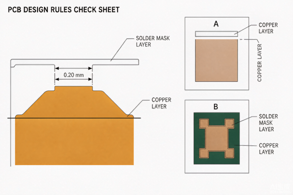
- Copper pour too close to the board edge. Large copper pours need at least 0.2 mm clearance from the outline. Rout any closer, and the copper can lift during profiling, pulling the solder mask off with it.
- Filled blocks used as pads. A filled block passes DRC but doesn’t generate solder-mask data. The block gets covered by solder mask, and the part won’t solder properly. Pads need to be real pads, not shapes.
If your files have any of these, a good DFM review catches them before fabrication — a cheap fix compared to re-spinning a board.
The Bottom Line
SMT quality inspection standards are only worth something if they’re specific. A supplier that can tell you the exact solder-ball limit, the exact overhang percentage, and the exact edge clearance is one that actually controls its process. The list above is the baseline we hold our own lines to.
Foire aux questions (FAQ)
A:What is the acceptable solder ball size in SMT assembly?
A solder ball is acceptable if its diameter is 0.13 mm or less, and it isn’t trapped in no-clean residue or covered by conformal coating. Anything larger is a reject.
A:What’s the difference between tombstoning and billboarding?
Both are placement defects on chip components. Tombstoning means one end lifts fully off the pad (always rejected). Billboarding means the part tips on its side; it’s acceptable only if the width-to-height ratio stays at 2:1 or less.
A:How much side overhang is acceptable on a chip component?
For rectangular or square chip terminations, the side overhang (A) must be ≤50% of the termination width (W) or the pad width (P). For cylindrical end caps, the limit is tighter — ≤25%.
A:What is the minimum copper-to-edge clearance in PCB design?
Keep large copper pours at least 0.2 mm away from the board outline. This prevents the copper from lifting during routing and keeps the solder mask intact.
A:Why shouldn’t filled blocks be used as PCB pads?
A filled block won’t generate solder-mask data, so the area gets covered by solder mask and the component can’t solder properly. Use a real pad instead.
À propos de nous

À propos de l'auteur
Andrew Zhan – Ingénieur R&D chez JKRGLO.com
Fort de plus de 14 ans d'expérience en ingénierie de R&D dans le secteur des circuits imprimés, Andrew Zhan apporte une expertise approfondie en matière d'optimisation de la conception des circuits et de mise en œuvre des principes de conception pour la fabrication (DFM). Il s'attache à transformer des exigences de conception complexes en solutions prêtes pour la production, en favorisant l'innovation technique tant pour la fabrication de prototypes que pour la production en série.
En étroite collaboration avec des équipes pluridisciplinaires et les clients, il veille à une validation rigoureuse de la qualité et à une communication technique fluide tout au long du cycle de vie du projet. Andrew s'engage à fournir des solutions de circuits imprimés fiables et hautement performantes qui dépassent systématiquement les attentes des clients.
Table des matières
Vous avez encore besoin d'aide ? Contactez-nous :
Vous avez besoin d'un devis pour un circuit imprimé (PCB) ou un assemblage de circuit imprimé (PCBA) ?
Étiquette :
les meilleurs fabricants de circuits imprimés
PCBA
PCB
IPC-A-610
SMT quality inspection standards