
PCBA Testing: What Each Method Catches, What It Misses, and How to Choose
Quick answer
PCBA testing checks a populated circuit board against defined electrical and functional requirements. A practical production plan combines inspection of the assembly with electrical checks and powered functional testing where required. Choose the methods from the defects and behaviors that must be detected, then confirm access, limits, records and failure handling before the build.
Test coverage is the set of faults, connections or functions a stated inspection or test program can evaluate under defined conditions. A list of installed machines is not a coverage statement.
A passing PCBA test result means the unit met the recorded checks and limits at that time. It does not prove every operating condition, every hidden joint or the product’s entire service life.
Two suppliers can both quote a tested assembly and mean different things. One may check appearance and shorts. Another may load firmware, exercise interfaces and record measurements by serial number. Comparing those offers as if the test scope were identical is an avoidable sourcing error.
The same ambiguity causes trouble on the line. A board that passes optical inspection can still carry the wrong resistor value. A board that boots can still have an untested input, an intermittent connection or a configuration problem. The answer is not to buy every available test. It is to decide what evidence each stage must provide.
This guide joins the method-selection question with the common-defect question: which fault are you looking for, how can the chosen method detect it, and what happens if it fails? For the wider build sequence, see the PCB assembly process.
What Is PCBA Testing, and How Is It Different From Inspection?
PCBA testing is the application of defined electrical or functional checks to an assembled printed circuit board to evaluate specified manufacturing faults or product behavior.
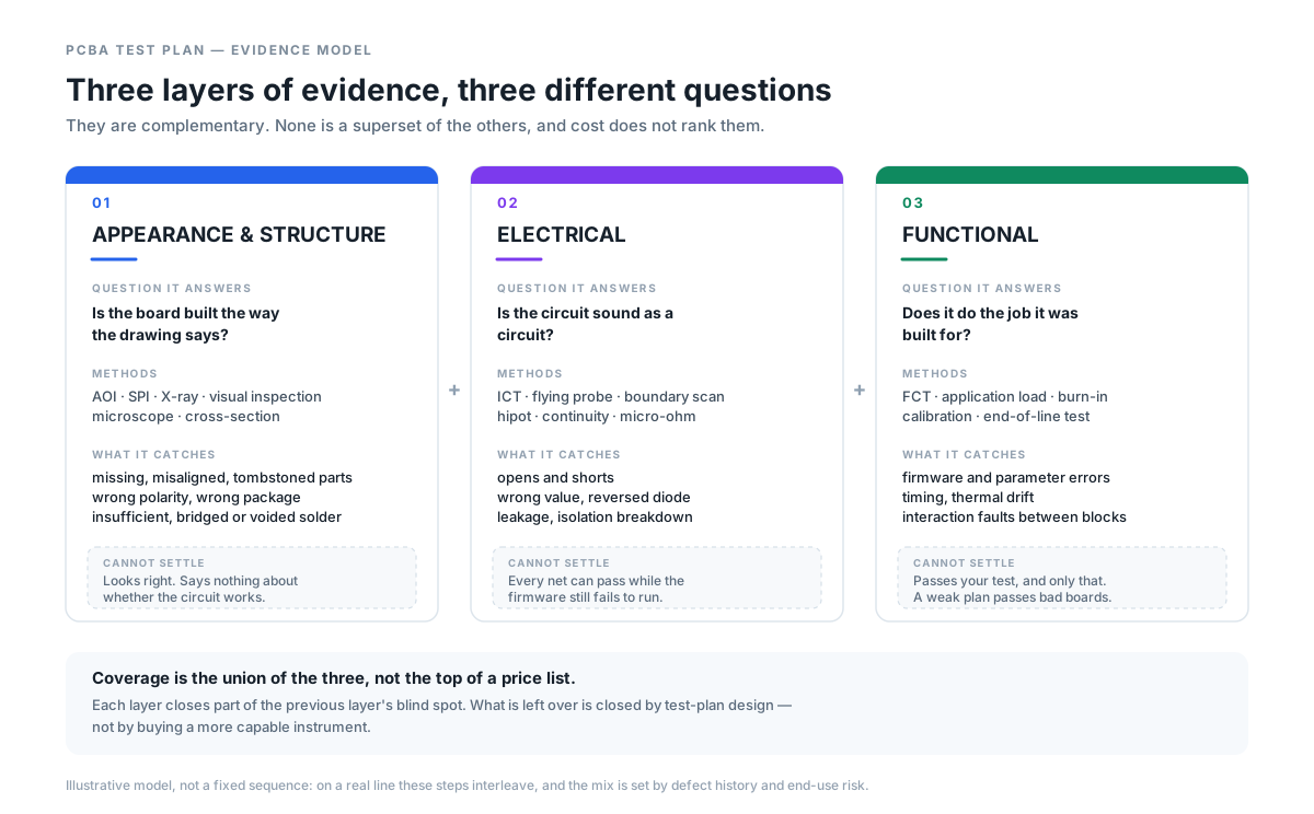
People often use testing as an umbrella term for every quality checkpoint. That is workable in a conversation, but the production plan needs more precision. Inspection observes a feature, image or measured structure. Electrical testing measures circuit responses or connectivity. Functional testing exercises powered behavior. The categories overlap in equipment, but the evidence is not interchangeable.
| Activity | Typical evidence | What it does not automatically establish |
|---|---|---|
| Assembly inspection | Images or measurements of paste, placement, visible joints or hidden structure | That every circuit function operates correctly |
| Electrical structural test | Measured values, continuity or fault indications on covered circuits | That every product mode has been exercised |
| Functional test | Powered responses against defined inputs, loads and limits | All physical workmanship or all lifetime failure mechanisms |
| Reliability qualification / screening | Results under a specified stress or qualification plan | That a short routine production check is equivalent |
Also separate bare-board electrical test from assembled-board test. A fabricator can verify a bare PCB against its electrical data before components are fitted. Assembly then introduces components, solder joints, programming and further handling. The earlier pass does not close those new risks.
A usable test statement names the unit, revision, method, limits and result. It also identifies what was not tested. That last part is important: an honest exclusion gives engineering something to assess. A promise of complete testing with no coverage detail does not.
For a buyer, the distinction changes the RFQ. Instead of asking for full testing, describe the required checks or ask the supplier to propose a coverage matrix. Give the product requirements and important failure modes so the proposal can be reviewed rather than guessed.
For engineering, the same distinction prevents a test station from becoming a substitute for design validation. A production test should be capable of identifying defined faults efficiently. Demonstrating that the design is fit for every claimed application needs its own evidence and qualification plan.
PCBA Test Methods: What Each One Can and Cannot Tell You
A layered PCBA test strategy combines complementary evidence so that visible defects, electrical faults and required operating behaviors are not treated as the same problem.
The comparison below describes roles, not guaranteed detection rates. Actual coverage depends on the assembly, available access, program, equipment and acceptance rules. A camera or probe can only evaluate what its setup allows it to observe or measure.
| Method | Main role | Useful for | Important limitation |
|---|---|---|---|
| SPI | Measure paste deposits before placement | Printing volume, area, height or alignment checks as supported | Does not inspect the final soldered joint |
| AOI | Inspect visible component and solder features | Missing/shifted parts, readable polarity and visible anomalies | Cannot fully observe hidden joints or prove electrical function |
| X-ray / CT | Examine internal or obscured structure | Selected hidden bridges, voids and structural features | Detectability depends on geometry/resolution; not a function test |
| ICT | Apply programmed electrical tests through suitable access | Covered shorts, opens, values and supported device checks | Access, parallel paths and program limits restrict coverage |
| Flying probe | Move probes to programmed electrical targets | Flexible electrical checks during development or changing builds | Contact access and cycle time still need verification |
| Boundary scan | Use supported device test structures | Certain digital interconnect checks with suitable devices and design | Does not cover arbitrary nets or all device behavior |
| FCT | Exercise the powered assembly | Specified rails, I/O, interfaces and application behavior | Untested modes and limits remain outside the result |
| Stress testing / screening | Apply an agreed exposure or sequence | Selected failure mechanisms under a defined plan | Not a universal substitute for normal inspection or qualification |
Do not turn this into a fixed ladder in which more expensive always means better. A test that cannot reach the important fault provides little value, regardless of its price. An inexpensive check that detects a likely assembly fault before powered testing may be highly useful.
A method name alone is not enough. Two functional stations can differ in loads, instrument resolution, software and operating modes. Two ICT programs can cover different nodes on the same design. Ask for the actual plan and the exclusions.
Use the table to organize a technical review. For every important requirement, identify at least the proposed evidence, where it is generated and who approves an exception. Where coverage is intentionally omitted, record the justification rather than allowing the omission to remain invisible.
Common PCBA Defects: Match the Symptom to the Evidence
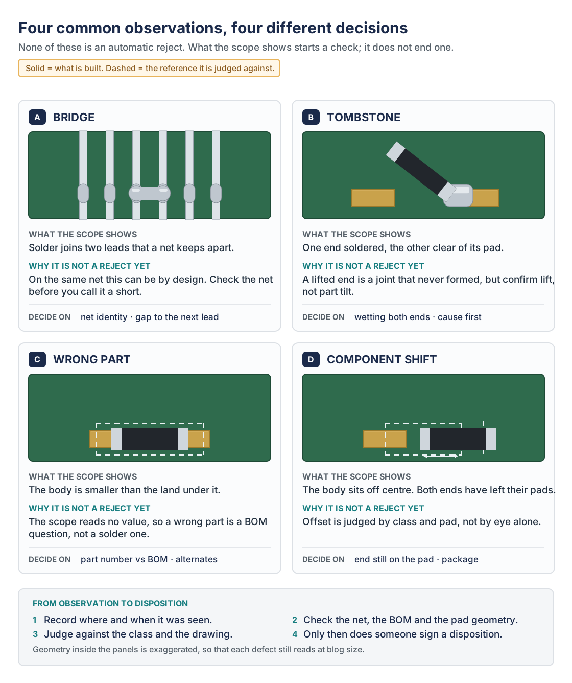
A PCBA defect is a condition that fails an applicable assembly, electrical or product requirement; a visible anomaly or a void is not automatically a reject without the relevant criteria.
Defects deserve their own section because the same symptom can have several causes. A dead rail might come from a bridge, an incorrect component, an open connection or a setup problem. Begin with a contained unit and a recorded observation, not an immediate change to the oven recipe.
| Defect or observation | Candidate detection route | What to investigate | Boundary / caution |
|---|---|---|---|
| Solder bridge | Visual/AOI where visible; suitable X-ray or electrical short check where hidden | Paste deposition, stencil/registration, placement and soldering conditions | A bridge beneath a package may not be optically visible |
| Tombstoned passive | Visual or AOI, with electrical evidence if required | Unequal wetting forces, pad/paste balance, component and thermal conditions | Do not attribute every case to one reflow setting |
| Open or insufficient joint | Visible inspection where accessible; electrical tests; suitable structural analysis | Paste, wetting, coplanarity, contamination and process history | A simple appearance check may miss an obscured discontinuity |
| Voiding observation | Appropriate X-ray views / CT if justified | Material, pad/aperture design, process and package guidance | Acceptance depends on package, location and agreed measurement |
| Wrong or missing component | BOM/placement review, AOI where distinguishable, electrical or functional checks | Material identity, feeder setup and released data | Similar packages can hide a wrong electrical value |
| Reversed polarity | AOI/visual marking where readable; supported electrical/function tests | Part interpretation, library and setup verification | Some polarity features are not optically accessible |
| Component shift | AOI/visual and downstream electrical evidence | Placement, paste, handling, board support and soldering | Choose the correction from evidence, not a generic fix list |
| Intermittent connection | Repeatable fault investigation, appropriate measurement and analysis | Mechanical/thermal conditions, joint or component damage, setup | A single passing run cannot dismiss the observation |
| Wrong firmware / configuration | Version verification and specified functional checks | Image control, programming and change effectivity | Correct soldering cannot establish the correct software |
The table is deliberately cautious about causes. Extending a preheat stage is not the universal remedy for voiding. Slowing a conveyor is not the universal remedy for placement shift. A change that helps one condition can move another feature outside its process window.
Preserve the fault evidence before rework. Record serial number, board revision, position, station result and relevant images. Otherwise an engineer may receive a repaired board and a story, but no way to verify the original failure or the effectiveness of the correction.
Use the agreed acceptance basis. A workmanship criterion, component recommendation and functional limit may address different questions. Where they conflict or leave a gap, resolve the specification before accepting or rejecting a lot.
This defect-to-method map absorbs the practical topic of the former common-defects article. It should remain a clearly titled section so readers seeking a particular defect do not have to work through the whole test-selection discussion.
SPI and AOI: Catch What Is Visible, Then Record the Reaction
Automated optical inspection compares visible assembly features with a programmed inspection model; the result depends on the views, references, limits and review rules used by that program.
SPI belongs before placement, where a printing issue can be investigated before it becomes a soldered assembly. Its value is not a universal percentage of defects prevented. Its value is a suitable measurement and a controlled reaction when the process leaves the approved conditions.
Ask which features are measured and how the recipe was approved. A board-wide average can conceal a difficult aperture. Review the feature that matters, the actual measurement and the action taken. The solder paste inspection guide explains that upstream checkpoint in more detail.
After placement or soldering, AOI may detect missing, shifted or reversed parts and visible joint anomalies, depending on what the setup can see. Three-dimensional measurement can add information, but it does not remove the need for a validated recipe or make opaque package bodies transparent.
Check the review path as carefully as the detection. Who resolves a call? What record remains if it is judged acceptable? Can an operator bypass a repeated call without authorization? A system that produces many alarms but records little about disposition is difficult to audit.
Distinguish a false call from a defect escape. A false call is an inspection indication resolved as acceptable under the applicable rules. An escape is an unacceptable condition that passes a checkpoint. Lowering a threshold to reduce nuisance calls may change both; evaluate relevant examples before releasing the revised program.
Where parts look alike, optical inspection may not determine electrical identity. A resistor with the right package but the wrong value may need supported electrical measurement or other evidence. That is why AOI belongs in a coverage matrix rather than standing in for all testing.
If a revision changes polarity marks, component height, mask color or placement, review whether the optical program remains valid. A familiar board name does not prove the current assembly is the one used to develop the recipe.
X-Ray and CT: Inspect Hidden Structure Without Overclaiming
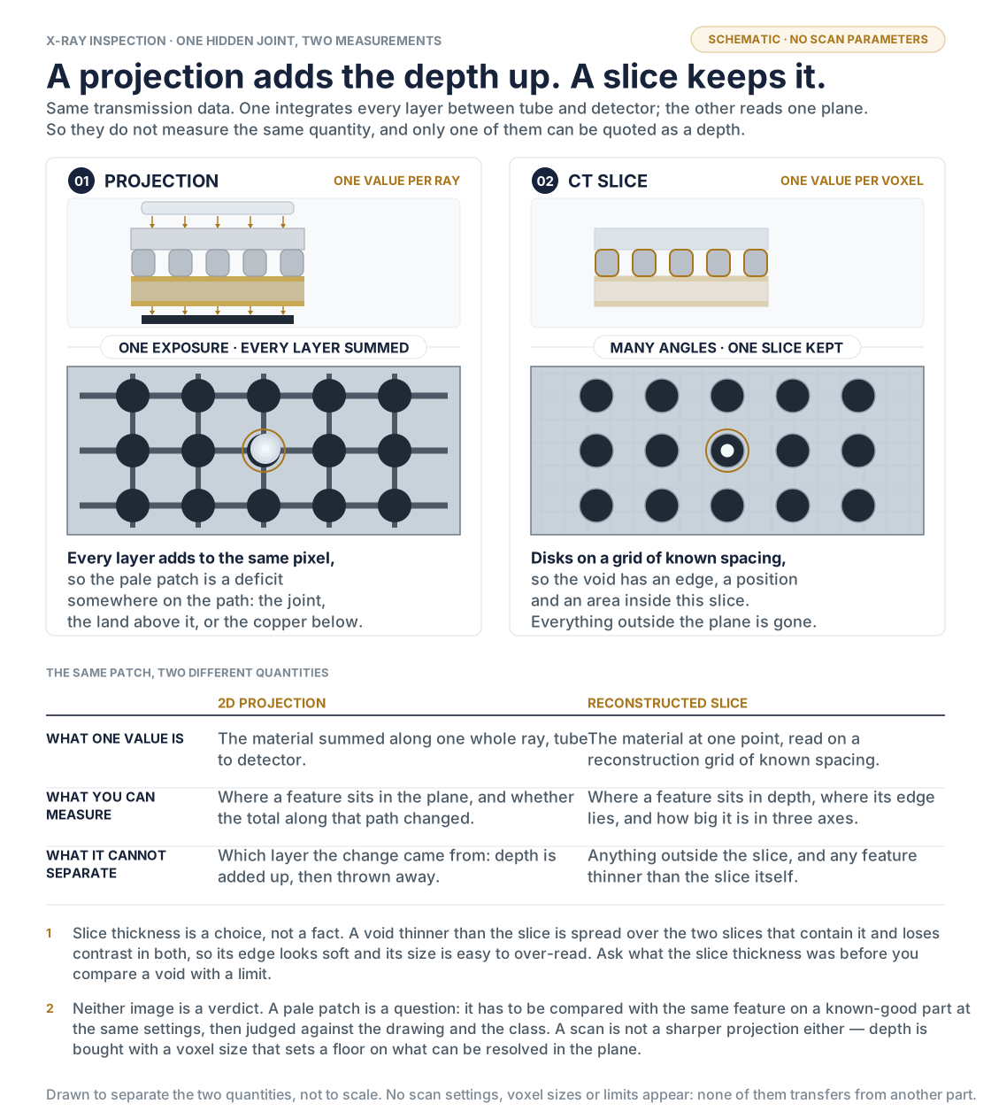
X-ray inspection evaluates features through differences in transmitted radiation, while CT reconstructs volumetric information from multiple projections; neither method directly proves the assembly’s electrical function.
Hidden-joint inspection is relevant when package bodies or overlapping structures prevent a suitable optical view. The method has to resolve the defect of interest. Ask which views are used, what may overlap and how the interpretation is checked.
A two-dimensional projection can be useful for some hidden solder observations. CT or another suitable technique may be justified when overlap or geometry makes that projection ambiguous. Do not make three-dimensional imaging a universal purchasing condition merely because the board contains a BGA.
| Question | Evidence to request | Avoid concluding |
|---|---|---|
| What fault is being sought? | Named feature and detection objective | One image proves every hidden joint sound |
| Can the view resolve it? | Representative views, method and limitations | All cracks or fine opens are always visible |
| How is voiding assessed? | Package-specific criterion and measurement definition | Projected area equals three-dimensional volume |
| Who decides acceptance? | Controlled limits, reviewer competence and disposition record | A supplier’s generic percentage overrides the contract |
Voiding is especially easy to oversimplify. The significance depends on joint geometry, location, function and the applicable requirements. A percentage without a defined measurement method and relevant criterion is not an acceptance rule.
Do not write that all BGA or thermal-pad joints must meet one fixed volume limit under IPC. Different package categories and documents have different scopes. Use the contractually applicable requirements and component guidance; verify a numerical clause when it is needed.
For a failed unit, relate the image to electrical symptoms and process history. Finding a visible internal feature is not always finding the root cause. A sound investigation tests whether the observation explains the failure and whether the proposed correction changes the result.
Our 3D X-ray and void inspection discussion provides a focused starting point. Product-specific criteria and validated methods should still govern the decision.
ICT vs Flying Probe: Compare Access, Coverage and Real Cost
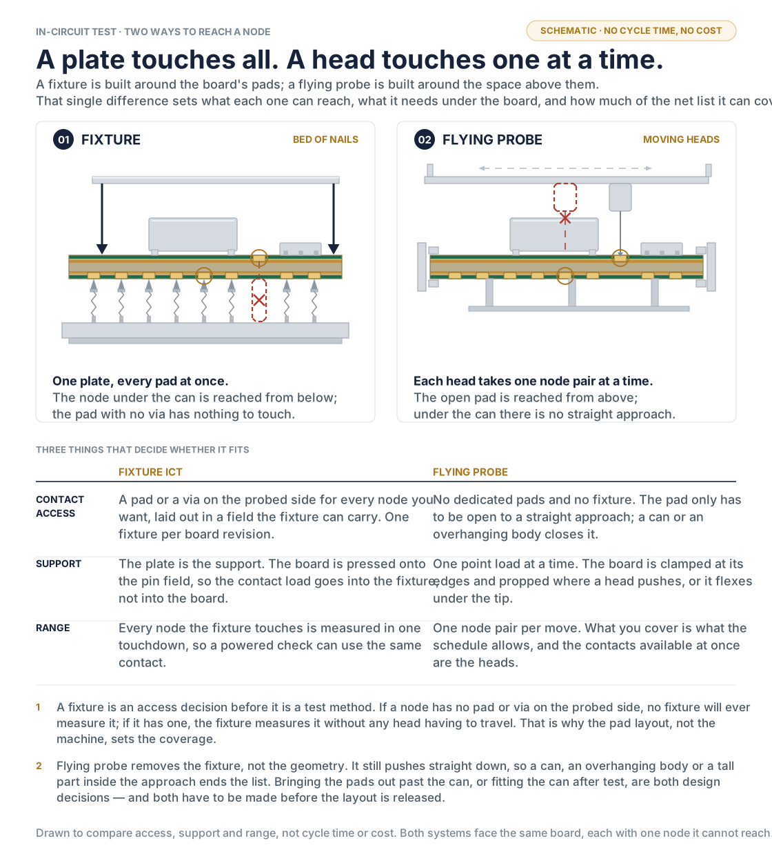
In-circuit testing applies programmed electrical measurements through suitable board access to evaluate covered assembly faults; flying probe testing uses moving contacts to reach programmed targets without the same dedicated bed-of-nails fixture arrangement.
The central question is whether both proposals detect the faults you need. An apparent cost advantage is meaningless if one program excludes an important network or component. Review the covered tests, not just the number of probe targets.
| Decision factor | Fixture-based ICT | Flying probe |
|---|---|---|
| Physical contact | Dedicated contact arrangement for the assembly | Moving probes with appropriate access and board support |
| Revision flexibility | May require fixture and program changes | Program changes may be easier, but access still matters |
| Cycle and throughput | Can be efficient for a stable supported production route | Movement and selected checks influence cycle time |
| Cost structure | Fixture, engineering, validation and maintenance | Programming, support, handling and recurring time |
| Best comparison basis | Required coverage on the released assembly | The same required coverage and release evidence |
Do not say flying probe is useless at volume or ICT is always uneconomical below a particular quantity. Product complexity, cycle time, design stability, mix and order pattern all affect the decision. Some assemblies justify a fixture early; others remain better suited to a flexible route.
Fixtureless does not mean no support, no tooling or no engineering. Moving probes still need safe contact targets, clearance, alignment and a way to hold the board. TAKAYA’s public materials describe programmed probing and supported measurements; they do not make every populated design accessible.
Parallel contact also does not mean every measurement is completed simultaneously. The tester architecture and program determine measurement sequencing. Ask for the quoted cycle on the actual test scope rather than deriving throughput from the probe count.
A simple economic comparison is total engineering and fixture cost plus recurring test cost over the expected build quantity. Include maintenance, handling, debugging, revisions and the chance that a fixture is retired early. Only compare totals after the coverage is acceptable.
For a stable design, confirm who owns and stores the fixture and who approves repairs or updates. For a changing design, confirm how revised data reaches the program and which regression checks are repeated. See the independent in-circuit test guide for more detail without duplicating that topic here.
Functional Testing and Boundary Scan Answer Different Questions
Functional testing applies defined power, stimuli, loads and observations to determine whether an assembly meets the selected operating requirements under the stated test conditions.
A board that powers up is not necessarily functionally tested. Define what boot success means, which rails are measured, which interfaces are exercised and which error states must be checked. A status LED can be useful evidence, but only for the behavior it actually represents.
Write an input, expected response and limit for each required check. State the firmware image, configuration, timing and environmental conditions where relevant. If the station uses a simulated load or loopback, record what that simulation represents and what remains unverified.
Keep programming verification visible. A successful flash operation is not always sufficient evidence that the right version and options are present. The required identity check belongs in the record, especially when one hardware revision supports several customer configurations.
| Check | Specify | Common gap |
|---|---|---|
| Power / sequencing | Supply conditions, current limits and required observations | Checking only one steady-state voltage |
| Communications | Interfaces, traffic, timing and error behavior | A loopback treated as complete end-use validation |
| Sensors / analog | Stimulus, calibration state and measurement limits | Accepting one nominal point for a range requirement |
| Programming | Approved image and identity/configuration verification | Logging only that a programming command completed |
| Supported digital interconnect | Boundary-scan architecture, access and covered faults | Assuming every net supports scan-based testing |
Boundary scan can add access to supported digital interconnects through device test structures. It requires compatible devices, design support, correct models and a suitable connection to the test system. It does not turn arbitrary analog circuits into observable scan networks.
Teradyne’s public Scan Pathfinder description identifies supported interconnect fault checks and access requirements. Keysight’s boundary-scan discussion also makes clear that a toolbox does not simply replace all ICT opens-and-shorts testing. These are complementary techniques, not interchangeable labels.
For products with safety-related outputs or hazardous energy, have the responsible engineers define interlocks and safe test conditions. Production operators should not improvise loads or probing on a live assembly. A test procedure needs to be safe as well as informative.
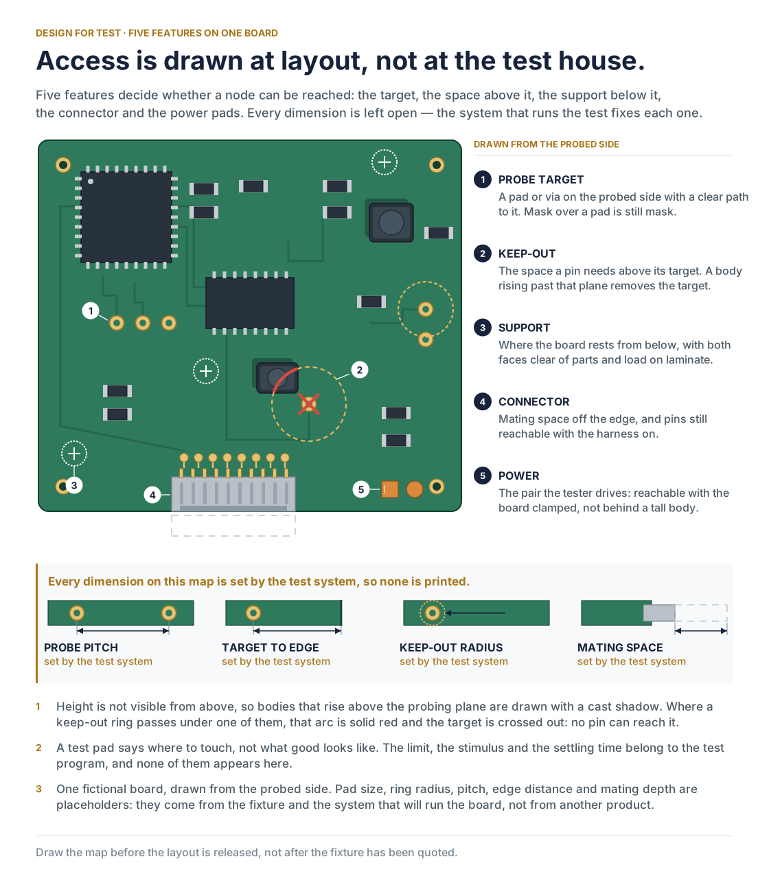
Design for Test Starts Before the Layout Is Released
Design for test, or DFT, is the planning of physical access, control, observability and test data so that the required checks can be performed safely and repeatably on the finished assembly.
Ask the proposed test provider to review access while changes are still affordable. A node visible on a schematic may be inaccessible under a connector or inside the final mechanical arrangement. A point reachable by hand on one sample may be unsuitable for a repeatable fixture.
| DFT item | Resolve before release | Why it matters |
|---|---|---|
| Targets and clearances | Tester/fixture-specific size, pitch, keep-out and side access | There is no universal 2.54 mm rule for every tester |
| Board support | Clamping, fiducials, warp and force considerations | Reliable contact must not damage the assembly |
| Power and control | Safe supply access, isolation and operating modes | The station needs a controlled initial state |
| Observability | Signals or outputs that demonstrate required behavior | An unobservable function may need a design change |
| Data package | Net-aware data, schematic, BOM, drawings and revisions | Gerber geometry alone may not define a complete electrical program |
| Firmware and limits | Released images, configuration and acceptance specification | A program cannot infer the product requirements from placement data |
Accessible targets must meet the chosen system’s requirements. Exposed pads, vias, leads or connector pins may be usable in some arrangements, but contact size, spacing, mechanical support and surface condition still need review. Do not simply remove mask from every possible point without engineering approval.
Consider circuits that interfere with measurement. Parallel paths, protective devices, limited power domains or sensitive inputs can affect what an electrical result means. The test developer may need isolation, special modes or an alternative observation rather than a different probe position.
Provide data under revision control. A BOM used for sourcing, a placement file used for setup and the schematic used for testing should identify a consistent baseline. Where differences are intentional, record them as approved variants, not discrepancies left for the test engineer to interpret.
El PCB design and manufacturing rules guide covers the earlier design baseline. For testability, add a project-specific access review to that process rather than relying on a generic spacing checklist.
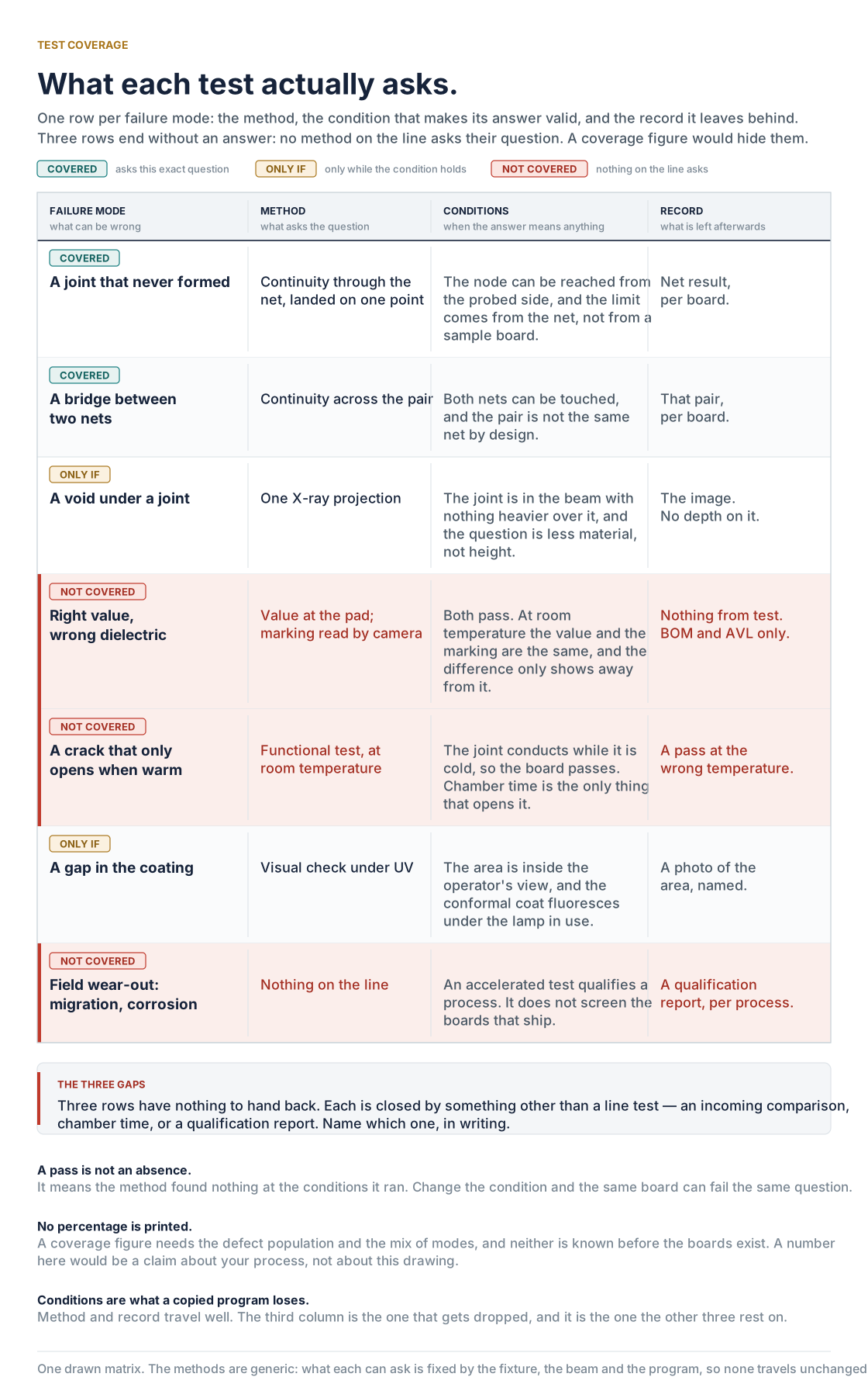
Build a Coverage Matrix Before Selecting the Final Route
A test coverage matrix links each defined failure mode or requirement to a detection method, test condition, acceptance basis and retained record, including justified gaps.
Start with what must not leave the factory. Then ask how each condition can be detected and where it is cheapest or safest to investigate. Early detection may reduce downstream work, but it does not justify removing later evidence needed for a different requirement.
| Requirement / risk | Proposed evidence | Condition to confirm | Record / owner |
|---|---|---|---|
| Visible wrong orientation | AOI or controlled visual check | The mark and feature are actually visible | Recipe/review and release owner |
| Hidden bridge | Appropriate structural or electrical check | Geometry and access support the proposed method | Inspection or measured result |
| Wrong passive value | Supported electrical measurement or justified alternative | Parallel paths and tolerance are accounted for | Value/limit/program revision |
| Firmware / variant identity | Controlled programming and identity check | Approved configuration matches the order | Image/configuration result |
| Interface operation | Defined functional exercise | Stimulus, load and required operating state are represented | Measured result / test owner |
| Intermittent fault risk | Product-specific analysis or validation plan | Stress and observations address the suspected mechanism | Investigation / qualification owner |
This is an illustrative structure, not a ready-approved plan for every board. Assign the actual methods to the actual design. Some faults may need more than one kind of evidence, and some requirements belong in design qualification rather than every-unit production testing.
Decide what runs on every unit, what is sampled and what is performed during qualification. Sampling is a risk decision with a defined plan, not an informal shortcut when the line is busy. Do not describe a sampled inspection as proof that every shipped unit received it.
Differentiate net coverage, component coverage, fault coverage and functional coverage. A high percentage of accessible nets does not mean the same percentage of product functions has been verified. If a supplier provides one coverage percentage, ask what the numerator and denominator contain.
For prototypes, prioritize learning and safe evidence collection. For repeat production, qualify the intended station and control the recurring route. A move from flying probe to ICT is a change to verify, not evidence that the original boards were untested.
Keep the matrix alive. A component substitution, firmware change or process change may affect the assumptions behind a check. Review the relevant rows instead of assuming the unchanged product name means unchanged test coverage.
Failed Units, Retesting and Root Cause: Preserve the First Result
Retesting is a repeat application of a defined test after an authorized event or disposition; it should preserve the original result and the reason for repeating the check.
A failing board should move into a controlled status, not back into the input queue until it happens to pass. Record the original result, identify the unit and contain affected material according to the plan. The next action depends on whether the evidence points to a product fault, contact problem, setup problem or uncertain result.
A fixture contact issue is possible. So is a real intermittent fault. The distinction needs evidence. Check contact condition, alignment, calibration status and station diagnostics under a defined procedure; do not silently erase a failure because the second run was green.
| Event | Required action | Evidence to retain |
|---|---|---|
| Initial fail | Identify and contain unit / affected scope | First measurement, limit, code and station revision |
| Suspected station issue | Verify setup under an authorized procedure | Diagnostic result and decision |
| Confirmed assembly defect | Authorize correction or other disposition | Location, cause evidence and rework record |
| Post-rework check | Repeat affected checks and agreed regression scope | New result linked to original failure |
| Recurring pattern | Review lot/process risk and corrective action | Counts, containment and effectiveness evidence |
Root cause is not the same as the defect name. Solder bridge describes the observed condition; it does not establish why the bridge occurred or why the inspection failed to contain it. Investigate both the creation mechanism and the escape mechanism when that distinction matters.
A process correction needs an effectiveness check. If a stencil or reflow change is made, define what subsequent data will show that the correction worked without creating a new problem. Avoid closing a corrective action solely because a report was issued.
Repaired units should remain traceable to the authorized disposition. The retest scope should account for what the intervention could affect, not merely repeat whichever check failed first. A local joint repair can disturb neighboring features; the appropriate review is product-specific.
For field failures that pass routine tests, preserve the use conditions and symptom. Consider operating states, thermal/mechanical exposure, firmware, components and the station itself. Do not jump from passed FCT to a diagnosis of micro-cracks or voids without supporting analysis.
Define Yield and Test Records So Two Suppliers Can Be Compared
First-pass yield is the fraction of units that pass a defined process or test scope on the first attempt; final yield may include units that pass after authorized correction or retest.
The definitions matter more than a headline percentage. A supplier reporting a first-pass functional result is not reporting the same thing as a supplier reporting final shipment acceptance after rework. Both records can be useful, but they answer different questions.
| Metric / record | Specify | Potential misunderstanding |
|---|---|---|
| First-pass yield | Scope, period, first attempt and denominator | Repaired passes quietly included |
| Final yield | Disposition and units counted | A high final result hides repeated rework |
| Defect count | Board, joint, component or opportunity basis | Different denominators compared as one rate |
| False calls / station issues | Definition and approved resolution categories | Station problems mixed with product defects |
| Unit record | Serial/lot, revisions, limits, measurements and status | A summary pass with no recoverable context |
| Retention / retrieval | Agreed duration, access and customer reporting | Records exist but cannot be tied to a shipment |
Ask for raw counts alongside the percentage. A small pilot can produce a dramatic percentage from one board. Large-volume trends and early builds should not be compared without the population and conditions behind them.
A useful unit record identifies the hardware and firmware baseline, station or program revision, applicable limits, time and result. Include measured values where required by the plan. The exact data scope and retention period belong in the agreement rather than being assumed.
Test limits need controlled ownership. If engineering changes a limit, preserve the justification, effective version and validation. Otherwise a trend can appear to improve simply because the pass boundary moved.
When asking a manufacturing partner for data, allow appropriate redaction of other customers’ identities while still requiring evidence for your own job. The PCBA supplier qualification guide explains how to sample records rather than relying on a capability brochure.
No single universal FPY target describes all products, stages and mixes. Set project requirements with a clear baseline and improvement process. Do not present an unsupported industry percentage as a promise for every build.
What Drives PCBA Test Cost? Scope Comes Before the Price
The cost of PCBA testing combines development and tooling with recurring execution, handling, maintenance and failure-disposition work for a defined coverage scope.
Request a quotation that separates one-time engineering from recurring test. A fixture, programming effort or custom load may be a development cost. Running a lengthy measurement sequence, handling boards and maintaining contacts continue through production.
| Cost element | Clarify | Why it changes the comparison |
|---|---|---|
| Engineering / fixtures | Program, hardware, validation, ownership and lead time | Two quotes may include different deliverables |
| Execution | Defined sequence, handling and cycle assumptions | A shortened sequence is not always an efficiency gain |
| Revision | Software, fixture and regression changes | Frequent design changes can alter total economics |
| Maintenance | Contacts, calibration, reference artifacts and storage | Upkeep does not disappear after fixture purchase |
| Failure handling | Diagnosis, rework authorization and retest | A low test price can exclude the work needed to release units |
Avoid choosing methods solely from unit-count bands. The decision depends on acceptable coverage, stable lifetime volume, cycle time, access and revision risk. The PCB assembly cost guide provides broader quotation context; the test scope still needs its own comparison.
If comparing fixture-based and moving-probe routes, calculate the economic crossover only after confirming both meet the requirement. Use actual quoted engineering and recurring costs, not a universal dollar range copied from a different product.
Agree who supplies reference units, firmware, loads, peripherals and expected responses. A supplier cannot validate an application-specific behavior from Gerbers alone. Missing test inputs can become schedule risk even when the assembly files are complete.
The lowest-cost defensible plan is not the plan with the fewest station names. It is the one that supplies the necessary evidence without redundant work, uncontrolled assumptions or unpriced gaps.

A PCBA Test Release Checklist for the Next Build
A test release package is the approved combination of requirements, programs, fixtures, references and disposition rules needed to run the intended production checks consistently.
Before the build, make sure the test developer, manufacturing team and product owner agree on the same baseline. Resolve open questions about limits, coverage and release authority before boards arrive at the station.
| Release item | Evidence needed |
|---|---|
| Requirements and coverage | Approved matrix, exclusions and applicable criteria |
| Data baseline | Consistent schematic, BOM, assembly data and firmware |
| Access and equipment | DFT review, support, safe connections and suitable instruments |
| Program qualification | Known acceptable references and relevant controlled fault checks where appropriate |
| Failure workflow | Containment, review, rework and retest permissions |
| Pilot / release | Representative results, open findings and authorized decision |
| Records | Traceable results, revisions, retention and retrieval agreement |
Reference assemblies and controlled fault examples can help qualify a station, but they also need control. A reference board can age or change. A deliberately introduced fault may not represent every natural failure. Use these artifacts to verify the stated checks, not to claim universal coverage.
For a JKRGLO project, provide the current manufacturing package, expected quantities, required behaviors and any existing test specification. Ask for a proposed inspection and electrical test route with exclusions, required inputs and responsibility for development.
Send the assembly and test requirements to JKRGLO for a scoped review before production. This is a request to establish project capability and responsibilities, not an assertion that every possible test is included as standard.
Technical references. Public equipment descriptions help establish method scope, not universal coverage: TAKAYA flying-probe product description; Teradyne Scan Pathfinder II FAQ; Keysight boundary-scan discussion. Apply the actual product specification and qualified station requirements to the build.
PCBA Testing: Frequently Asked Questions
1. What is PCBA testing?
PCBA testing applies defined electrical or functional checks to an assembled board. In a wider quality plan, it is combined with inspections such as SPI, AOI and suitable X-ray where needed. The approved scope should identify the faults and behaviors checked, the limits and the records retained.
2. What is the difference between PCB and PCBA testing?
Bare-board PCB testing checks the fabricated interconnect before assembly. PCBA testing addresses the populated board, including components, solder connections, programming and required operation. A bare-board pass does not verify work added during assembly.
3. Is AOI enough to test a PCBA?
Not generally. AOI evaluates features visible to its programmed imaging setup. It does not fully inspect hidden joints or prove electrical function. Determine which electrical and functional checks the product requires rather than assuming an optical pass closes every risk.
4. What are the common PCBA defects?
Common assembly concerns include solder bridges, tombstoned or shifted components, opens, insufficient joints, wrong parts and reversed polarity. Voiding and contamination observations need the applicable acceptance criteria. Programming or configuration errors can also make a physically correct board unsuitable for shipment.
5. Is ICT better than flying probe?
Neither is universally better. Compare required coverage, access, design stability, recurring volume, cycle time and total cost. Fixture-based ICT can be attractive for stable recurring work; moving probes can offer flexibility. The actual program and assembly determine the result.
6. Does a flying-probe test need dedicated test pads?
Not always; suitable accessible vias, leads, pads or contacts may be usable depending on the equipment and design. Targets still need adequate contact geometry, clearance and support. Confirm the access plan with the test provider before release.
7. Does every BGA board need CT inspection?
No. Choose a method that can resolve the relevant feature and defect. Some questions can be addressed with suitable projection views or electrical evidence; others need more detailed imaging or analysis. Agree the inspection objective and limits rather than imposing one method on every package.
8. Can functional testing detect every defect?
No. Functional testing checks the specified behaviors under the programmed conditions. Untested modes, intermittent mechanisms and some structural defects may remain outside its coverage. Define the scope and combine it with other evidence where required.
9. Why can a board pass testing and fail later?
A fault may lie outside the tested conditions, arise intermittently or develop after exposure. Programming, components, environment and the station itself can also matter. Preserve the symptom and investigate; a later failure does not by itself establish one particular solder-joint cause.
10. Should a failed board simply be tested again?
Only under an authorized retest procedure that preserves the original result and records the reason. Verify suspected station problems, contain product defects and link any rework to the subsequent checks. Repeating until pass is not a controlled release method.
11. What files are needed for PCBA test development?
Provide consistent schematic and net-aware design data, controlled BOM, assembly information, firmware and the product test requirements. Include expected responses, limits and known exclusions. Geometry files alone may not provide the connectivity or functional intent needed for a complete program.
12. How much does PCBA testing cost?
Cost depends on development, fixtures, access, sequence, handling, recurring cycle time, maintenance and failure handling. Ask for a separated quote at the agreed coverage. There is no universal unit price or fixed production quantity at which one method becomes mandatory.

Acerca del autor
Andrew Zhan – Ingeniero de I+D en JKRGLO.com
Con más de 14 años de experiencia en ingeniería de I+D en el sector de las placas de circuito impreso (PCB), Andrew Zhan aporta una amplia experiencia en la optimización del diseño de circuitos y la implementación de prácticas de fabricación (DFM). Se centra en convertir requisitos de diseño complejos en soluciones listas para la producción, impulsando la innovación técnica tanto para la fabricación de prototipos como para la producción en serie.
En estrecha colaboración con equipos multidisciplinares y con los clientes, garantiza una rigurosa validación de la calidad y una comunicación técnica fluida a lo largo de todo el ciclo de vida del proyecto. Andrew se compromete a ofrecer soluciones de placas de circuito impreso (PCB) fiables y de alto rendimiento que superen constantemente las expectativas de los clientes.
Índice
¿Aún necesitas ayuda? Ponte en contacto con nosotros:
¿Necesitas un presupuesto para una placa de circuito impreso (PCB) o un conjunto de placa de circuito impreso (PCBA)?
 English English English
 Deutsch
 Français
 Italiano
 Español
 日本語
 한국어 English English English Deutsch Français Italiano Español 日本語 한국어