
How Do Circuit Boards Work? A Complete Guide to PCB Fundamentals, Components, Manufacturing & Space-Grade Applications
Opening Introduction
1. What Is a Printed Circuit Board (PCB)?
It is important to distinguish between two commonly confused terms:
- Bare PCB: The blank board with only copper traces, solder mask, and silkscreen — no electronic components attached. This is the base product manufactured by PCB fabricators.
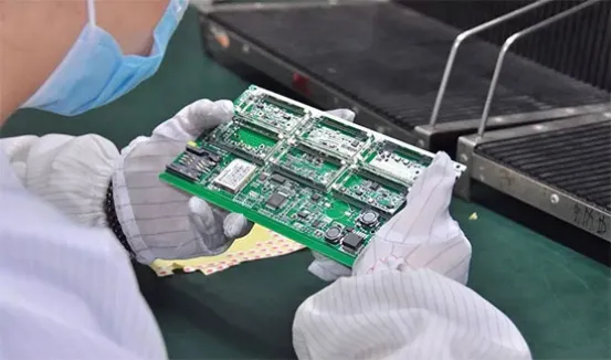
- PCBA (Printed Circuit Board Assembly): The fully populated board with all electronic components soldered into place, ready to be powered on and perform its intended function.Every circuit board’s core purpose is twofold: to physically hold electronic components in place, and to electrically connect them in a precise, predetermined pattern so the circuit can execute its designed function.
2. The Layered Anatomy of a Standard PCB
Most modern PCBs are built as stacked layers, each serving a specific purpose. Even simple double-sided boards follow this standard structure, while high-complexity industrial boards can have 20 or more layers.

2.1 Substrate (Base Material)
The substrate is the rigid or flexible core of the board, made from non-conductive insulating material. The most common industrial-grade substrate is FR-4 fiberglass epoxy, which offers excellent mechanical strength, heat resistance, and electrical insulation at a low cost. For flexible boards, polyimide (Kapton) is used, while aluminum metal core substrates are preferred for high-power LED and thermal management applications.
The substrate provides structural rigidity and physically separates conductive layers to prevent unintended short circuits.
2.2 Copper Conductive Layers
Thin sheets of pure copper foil are bonded to one or both sides of the substrate (and to inner layers for multi-layer boards). These copper layers are then chemically etched away to leave the precise network of traces, pads, and continuous planes that carry electrical current and signals.
Copper is the universal choice for conductive layers because of its excellent electrical conductivity, low cost, and strong bonding ability with solder. The thickness of the copper layer (measured in ounces per square foot) is selected based on how much current the board needs to carry.
2.3 Solder Mask Layer
Coated over the top and bottom copper layers is a protective polymer layer called solder mask, most commonly green in color.Solder mask serves three critical functions:
- It insulates copper traces from accidental contact with other conductive materials, preventing short circuits.
- It protects copper from oxidation, corrosion, and environmental damage over the board’s lifespan.
- It prevents solder from spreading to unintended areas during assembly, ensuring solder only bonds to exposed component pads.
2.4 Silkscreen Layer
The topmost layer is the white silkscreen, which is printed with text, symbols, and reference designators. Silkscreen markings help assembly technicians place components correctly, and help engineers troubleshoot finished boards by labeling component polarities, test points, board part numbers, and connector positions.
3. Key Electronic Components & Their Functions

| Component Type | Category | Core Function | Common Applications |
|---|---|---|---|
| Integrated Circuit (IC / Microchip) | Active | The "brain" of the circuit: contains millions of transistors to process data, execute logic, and control system functions | Microprocessors, memory chips, power management ICs |
| Resistor | Passive | Regulates and limits electrical current, divides voltage, and sets signal levels | All circuit types, current limiting, voltage division |
| Capacitor | Passive | Stores and releases electrical charge, filters out noise, and stabilizes voltage supply | Power supply circuits, signal filtering, IC decoupling |
| Diode | Active | Allows electrical current to flow in only one direction; LEDs are a variant that emits light | Reverse polarity protection, lighting, voltage regulation |
| Connector | Mechanical | Creates a physical interface between the PCB and external devices, power sources, or other boards | USB ports, power jacks, board-to-board connectors |
| Crystal Oscillator | Passive | Generates a precise, stable clock signal to synchronize all circuit operations | Microcontrollers, communication devices, timing circuits |
| Transformer | Passive | Steps up or steps down AC voltage, and provides electrical isolation between circuits | AC power supplies, high-voltage circuits |
4. How Circuit Boards Actually Work: Electrical Flow & Signal Logic
- Power Input & Regulation: Electrical power enters the board through a connector or battery terminal. It first passes through protection circuits (fuses, reverse-polarity diodes) and voltage regulators, which convert the raw input voltage to the exact levels required by different components (e.g., 5V for USB peripherals, 1.8V for microchips).
- Power Distribution: Copper power planes (large, continuous areas of copper) distribute regulated voltage across the board to every component that needs power. Matching ground planes provide a common low-resistance return path for all current, reducing electrical noise and improving signal stability.
- Signal Processing: Input signals (from sensors, buttons, or data connectors) travel along copper traces to active components like microcontrollers or ICs. The integrated circuit processes the signal according to its programmed logic — for example, converting a button press into a command to turn on a display.
- Signal Output: Processed output signals travel through additional traces to output components: displays, speakers, motors, or data transmission connectors.
- Controlled Path Design: Every trace is engineered with a specific width, length, and spacing to ensure the correct amount of current flows, and that high-speed signals do not interfere with each other (a problem called crosstalk).
For complex multi-layer boards, dedicated signal layers, power planes, and ground planes are stacked and separated by insulating substrate, allowing thousands of connections to fit in a small space without performance degradation.
5. Component Mounting Technologies: Through-Hole vs. Surface Mount
Components are attached to PCBs using two primary assembly methods, each with its own advantages and ideal use cases.

Through-Hole Technology (THT)
The older of the two methods, through-hole assembly involves drilling holes through the entire PCB, inserting component leads through the holes, and soldering the leads to copper pads on the opposite side.
- Pros: Extremely strong mechanical bond, ideal for components that experience physical stress (connectors, large capacitors, transformers). Easy to manually solder and rework.
- Cons: Drilling adds production cost; limits routing space on both sides of the board; not suitable for miniaturized, high-density designs.
Surface Mount Technology (SMT)
The dominant modern assembly method, SMT uses components designed to sit directly on the surface of the PCB, with no drilled holes required. Components are placed by high-speed pick-and-place machines and soldered via controlled reflow ovens.
- Pros: Supports extreme miniaturization, fully automated for high-volume production, allows components on both sides of the board, delivers better high-frequency and signal performance.
- Cons: Ultra-small components are harder to rework manually; requires precision automated assembly equipment.
6. Industrial PCB Manufacturing: From Design File to Finished Board
- DFM (Design for Manufacturability) Check: Engineers review the Gerber design files to identify potential manufacturing defects, spacing violations, or drill errors before production begins. This step drastically reduces scrap rates and improves production yield.
- Inner Layer Etching: For multi-layer boards, inner copper layers are first coated with photoresist, exposed to UV light through a precision film mask, and chemically etched to remove unwanted copper, leaving only the trace pattern.
- Layer Lamination: All inner layers are stacked with prepreg (epoxy bonding material) and outer copper foil, then heated and pressed under high pressure to fuse the layers into a single solid board.
- Drilling: High-precision CNC drills create through-holes, vias, and mounting holes in the board with micron-level accuracy.
- Copper Plating: The drilled holes are electroplated with copper to create conductive connections between layers.
- Outer Layer Etching & Solder Mask Application: The outer copper layers are etched to create the final trace pattern, then coated with solder mask and heat-cured.
- Surface Finish: Exposed copper pads are plated with a protective finish (HASL, ENIG, OSP, etc.) to prevent oxidation and ensure reliable solderability during assembly.
- Silkscreen Printing & Final Electrical Testing: Silkscreen markings are printed, and every board undergoes electrical testing (flying probe or bed-of-nails) to confirm there are no open or short circuits.
7. Common PCB Types & Their Use Cases (Including Space-Grade Electronics)
Not all circuit boards are built the same. Different substrate materials, layer counts, and construction methods are engineered for specific operating environments — from consumer devices to deep space missions.
Rigid PCBs
Flexible PCBs (Flex PCBs)
Metal Core PCBs (MCPCB)
High-Frequency / RF PCBs
Space-Grade / Aerospace PCBs
- Built with high-temperature, radiation-resistant substrate materials
- Designed with redundant circuits to prevent single-point failures
- Undergo rigorous qualification testing for thermal cycling, vibration, and radiation tolerance These are the circuit boards that power satellites, space telescopes, and Mars rovers — truly electronics beyond Earth.
8. Common PCB Failures & How to Prevent Them
Even well-designed circuit boards can fail if manufactured or operated incorrectly. The most common failures include:
Short Circuits: Two adjacent copper traces accidentally connect, causing excess current flow and potential component damage.
- Prevention: Follow minimum trace spacing design rules; use proper solder mask coverage; control for conductive debris during assembly.
Open Circuits: A trace breaks or a solder joint fails, interrupting current flow.
- Prevention: Ensure adequate trace width for the intended current load; use high-quality solder materials; strictly control reflow temperature profiles.
Overheating: High-power components generate too much heat, damaging the board substrate or nearby components.
- Prevention: Use copper pours and thermal vias to dissipate heat; select appropriate substrate materials for high-power designs.
Signal Integrity Issues: High-speed signals experience noise, crosstalk, or signal attenuation.
- Prevention: Follow controlled impedance design rules; use solid ground planes to isolate signals; keep high-speed trace runs short and away from noise sources.
9. The Future of Circuit Board Technology
As electronics continue to evolve, PCB technology is advancing to meet new demands for smaller size, higher performance, and greater sustainability:
HDI (High-Density Interconnect) PCBs: Use laser-drilled micro-vias and ultra-fine trace widths to pack far more connections into smaller spaces, enabling smaller, more powerful mobile and wearable devices.
Embedded Components: Resistors, capacitors, and even simple ICs are embedded inside the PCB layers, saving surface space and improving electrical performance.
Eco-Friendly PCBs: New biodegradable substrate materials and lead-free, low-temperature solders reduce the environmental impact of electronic waste.
3D-Molded Interconnect Devices (3D-MIDs): Injection-molded plastic parts with integrated conductive traces, combining mechanical structure and electrical circuitry in a single component.
Final Thoughts
Circuit boards are the unsung foundation of every modern electronic device, from the phone in your pocket to the satellites orbiting Earth. Their seemingly simple layered structure hides a remarkable level of engineering precision, where every trace width, pad size, and layer placement is carefully designed to deliver reliable electrical performance.
Understanding how circuit boards work is the first step to designing better products, selecting the right manufacturing partner, and avoiding costly design mistakes. Whether you’re building a simple prototype or a high-reliability aerospace system, working with an experienced PCB manufacturer and assembly partner ensures your boards will perform as designed — even in the most extreme environments.


