
What is Surface Mount Technology (SMT)? A Complete Guide to Process, Advantages, Defects & Best Practices
Opening Introduction
1. What is Surface Mount Technology (SMT)?
Components designed for SMT are called Surface Mount Devices (SMDs). They are manufactured with short, flat leads or exposed terminal pads that sit directly on copper solder pads on the PCB surface. Solder paste holds components temporarily in place before permanent soldering via reflow ovens.

Common SMT-Related Terminology
The industry uses a set of standard abbreviations for different parts of the SMT ecosystem:
SMD (Surface-Mount Device): Any electronic component designed for surface mounting
SMA (Surface-Mount Assembly): The completed assembly of SMD components on a PCB
SMC (Surface-Mount Component): Synonymous with SMD, referring to individual parts
SMP (Surface-Mount Package): The physical packaging format of an SMD (e.g., 0402, BGA, QFN)
SME (Surface-Mount Equipment): Machinery used for SMT production, such as pick-and-place machines
Unlike through-hole technology (THT), which requires drilling holes through the entire board, SMT leverages both sides of the PCB for component placement, enabling far higher circuit density in smaller form factors.

2. A Brief History of SMT Evolution
1960s: Early Origins: IBM first pioneered a precursor to SMT called “planar mounting” for mainframe computer circuits, replacing bulky through-hole parts with flat-mounted components to save space.
1980s: Mainstream Adoption: As consumer electronics like portable radios and early personal computers hit the market, SMT moved from niche aerospace use to mass production. By 1986, SMDs held only 10% of the electronics market, but adoption accelerated rapidly.
1990s: Industry Dominance: By the early 1990s, SMT had become the default assembly method for most electronic products, driven by improved automation equipment and standardized component packages.
2000s to Present: Extreme Miniaturization: Component sizes have shrunk from standard 1206 packages to 0402, 0201, and even 01005 (0.4mm × 0.2mm) packages. Advanced packages like BGAs, QFNs, and flip-chip technology have pushed density even higher for semiconductor applications.
3. Core Advantages of SMT Over Through-Hole Technology
1. Unmatched Miniaturization & Circuit Density
SMT components are a fraction of the size of equivalent through-hole parts, and they can be placed on both sides of a PCB. This allows 3–10 times more components per square inch of board space, making compact devices like smartwatches, wireless earbuds, and smartphone motherboards possible. The smallest SMD passives (01005 package) are smaller than a grain of table salt.
2. High Automation & Lower Production Cost
Nearly the entire SMT process is automated, from solder paste printing to component placement and inspection. High-speed pick-and-place machines can place 30,000–100,000 components per hour with sub-millimeter accuracy. This drastically reduces labor costs, speeds up production, and minimizes human error compared to manual through-hole assembly.
3. Superior Electrical & High-Frequency Performance
SMT components have very short or no lead lengths, which reduces parasitic capacitance and inductance in the circuit. This results in better signal integrity, less electromagnetic interference, and more stable performance at high frequencies — a critical advantage for RF, 5G, and high-speed digital circuits.
4. Improved Mechanical Reliability
SMT solder joints form a strong, uniform bond across the entire component pad, rather than just around a single lead. This makes SMT assemblies more resistant to vibration and mechanical shock, which is essential for automotive, aerospace, and portable electronics applications.
5. Greater Design Flexibility
4. Step-by-Step SMT Assembly Process
Step 1: Solder Paste Printing & SPI Verification
The process begins with applying solder paste — a uniform mixture of tiny solder alloy spheres (typically SAC305: 96.5% tin, 3% silver, 0.5% copper) and flux — to exact component pad locations.
- A precision laser-cut stainless steel stencil is aligned over the PCB panel.
- A mechanical squeegee spreads solder paste across the stencil, depositing a controlled thickness of paste only on exposed copper pads.
- After printing, a Solder Paste Inspection (SPI) machine uses 3D scanning to verify paste volume, height, and alignment, catching printing errors before components are placed.
Consistent paste application is the single biggest factor in preventing SMT defects.

Step 2: High-Speed Component Placement
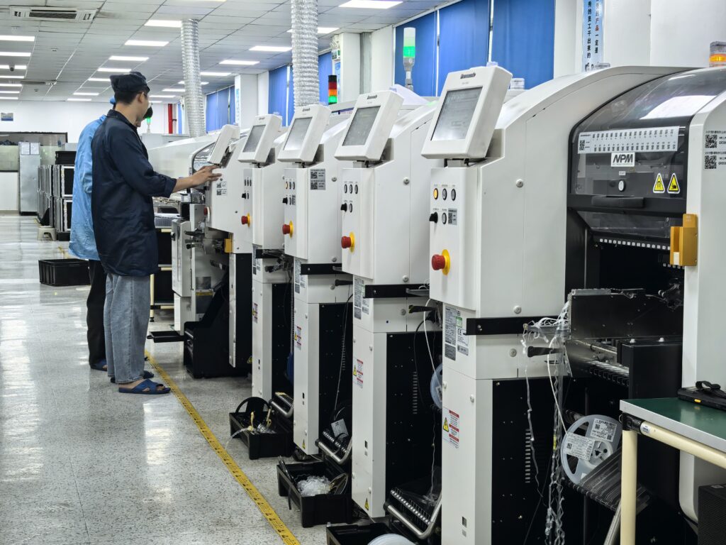
After paste printing, the PCB panel moves to pick-and-place machines, the workhorses of SMT production.
- Machines use precision vacuum nozzles to pick individual SMD components from reels, trays, or tubes.
- On-board vision systems align each component to within ±0.01mm accuracy before placing it onto the solder paste.
- Components are placed in pre-programmed positions, with correct polarity and orientation.
High-speed lines can place tens of thousands of components per hour, with support for packages as small as 01005 and as complex as fine-pitch BGAs.
Step 3: Reflow Soldering
With all components in place, the PCB panel travels through a reflow oven on a conveyor belt to form permanent solder joints. The oven uses multiple independent heating zones to follow a precise temperature profile:
- Preheat Zone: Gradually raises board temperature to avoid thermal shock and activate flux chemistry.
- Soak Zone: Holds temperature at ~150–180°C to allow flux to clean pad surfaces and remove oxides.
- Reflow Zone: Heats the board above the solder melting point (~217°C for SAC305), peaking at 240–250°C to form liquid solder bonds.
- Cooling Zone: Gradually lowers temperature to solidify joints evenly and reduce internal stress.
For double-sided SMT boards, the process is repeated for the second side with adjusted temperature parameters to prevent re-melting of first-side joints.
Step 4: Post-Solder Inspection & Quality Control
After reflow, every board undergoes inspection to identify soldering defects:
- Automatic Optical Inspection (AOI): High-resolution cameras scan the board and compare solder joint appearance to pre-programmed good-joint standards. AOI catches visible defects like bridging, tombstoning, and missing components at high speed.
- X-Ray Inspection: Used for hidden solder joints on BGA, QFN, and flip-chip packages, where connections sit under the component body and cannot be seen optically. X-rays detect voids, cracks, and misaligned balls.
- Manual Inspection: Used for low-volume prototypes or to confirm defects flagged by automated systems.

Step 5: Post-Assembly Cleaning & Rework
- Flux residue left from soldering is removed with a high-pressure deionized water wash to prevent corrosion and improve long-term reliability.
- Defective boards are sent to skilled rework technicians, who use specialized hot air stations to remove and replace faulty components without damaging the board.
5. Common SMT Defects: Causes & Prevention
Even with automated processes, SMT defects can occur from poor design, incorrect process parameters, or low-quality materials. Below are the most frequent defects and how to avoid them:

- Appearance: One end of a small passive component lifts off the pad and stands upright like a tombstone.
- Cause: Uneven heating or uneven solder paste volume causes one end of the part to reflow earlier and pull the component upward.
- Prevention: Ensure symmetrical pad design and uniform paste volume; optimize reflow temperature profile for even heating.
- Appearance: Excess solder connects two adjacent pads, creating an unintended short circuit.
- Cause: Excessive solder paste volume, misaligned stencil, or too fine a pitch between pads.
- Prevention: Verify stencil alignment; adjust paste volume; maintain minimum pad spacing per IPC standards.
- Appearance: Dull, grainy, or rough solder joints with poor wetting to the pad.
- Cause: Insufficient reflow heat, contaminated pad surfaces, or expired solder paste.
- Prevention: Calibrate reflow oven temperatures regularly; use fresh, properly stored solder paste.
- Appearance: Small spherical solder particles scattered around component pads.
- Cause: Excess paste volume, rapid heating during reflow, or contaminated paste.
- Prevention: Optimize stencil aperture size; control preheat ramp rate.
- Appearance: Air gaps inside BGA solder balls, visible only via X-ray.
- Cause: Outgassing from flux or PCB surface contamination during reflow.
- Prevention: Use high-quality solder paste; optimize reflow soak time to allow flux to outgas fully.
6. SMT vs. Through-Hole Technology: How to Choose
While SMT is dominant, through-hole technology still has important use cases. The table below compares the two methods to help you select the right approach:
| Factor | SMT | THT |
|---|---|---|
| Component Size | Very small (01005 and up) | Large, bulky parts |
| Circuit Density | Very high, supports double-sided placement | Low, single-sided only for most designs |
| Production Speed | Fast, fully automated | Slower, often requires manual insertion |
| Mechanical Strength | Good for vibration | Excellent for high-stress parts |
| High-Frequency Performance | Superior | Poor due to long lead inductance |
| Rework Difficulty | Requires specialized tools | Simple with basic soldering iron |
| Best For | Consumer electronics, high-density circuits, RF/high-speed designs | Power connectors, large capacitors, transformers, high-stress industrial parts |
Most modern boards use a mixed-technology approach: SMDs for the majority of components, with through-hole parts reserved for connectors and high-power components that need extra mechanical strength.
7. DFM Best Practices for Reliable SMT Assembly
Design for Manufacturability (DFM) is the single most effective way to reduce SMT defects and lower production costs. Follow these guidelines when laying out your SMT design:
Add fiducial marks: Place 3 or more global fiducial markers on each PCB panel to help pick-and-place machines align accurately. Add local fiducials around fine-pitch ICs and BGAs.
Use symmetrical pad designs: For passive components, ensure pads are identical in size and shape to prevent tombstoning.
Add thermal relief pads: Connect large copper planes to component pads with thermal relief spokes to prevent uneven heating during reflow.
Maintain minimum clearance: Leave enough space between components for inspection and rework. Avoid placing small parts directly next to tall components that can block heating during reflow.
Standardize component orientations: Align polarized components (diodes, ICs, capacitors) in the same direction where possible to reduce placement errors and simplify inspection.
Avoid ultra-small packages unless necessary: 0402 and 0603 passives have much lower defect rates than 0201 or 01005 packages, with minimal size tradeoff for most applications.
8. Future Trends Shaping SMT Manufacturing
SMT technology continues to evolve to meet the demands of next-generation electronics. Three key trends are redefining the industry in 2026 and beyond:
AI-Powered Inspection: Machine learning algorithms are being integrated into AOI and X-ray systems, reducing false defect detection rates by 60%+ and cutting manual review time dramatically.
Low-Temperature Solder Alloys: New low-melting-point solder formulations reduce reflow temperatures by 20–30°C, cutting energy use and reducing thermal damage to sensitive components and flexible substrates.
Advanced Heterogeneous Integration: SMT lines are being upgraded to handle chip-scale packages (CSPs), flip-chip components, and miniaturized system-in-package (SiP) designs, enabling even higher circuit density for AI edge devices and wearables.

Final Thoughts
Surface Mount Technology is the foundation of modern electronics manufacturing, enabling the compact, high-performance devices we use every day. Understanding the SMT workflow, common defects, and design best practices allows engineering and product teams to optimize their designs, reduce production costs, and build more reliable products.
The key to successful SMT production is partnering with an assembly provider that combines advanced automation equipment, rigorous quality control, and DFM expertise to catch issues early and deliver consistent results.
If you are preparing for an SMT assembly project, start with a free design for manufacturability review to identify cost-saving opportunities and potential defects before production begins.

