
What is an In-Circuit Test (ICT)? The Gatekeeper of PCBA Quality
Opening Introduction
Often called the “bed of nails” test, ICT is considered the gold standard for high-volume quality assurance in Printed Circuit Board Assembly (PCBA). Let’s dive into what an In-Circuit Test is, how it works, what it checks, and whether your hardware project needs it.
What is an In-Circuit Test (ICT)?
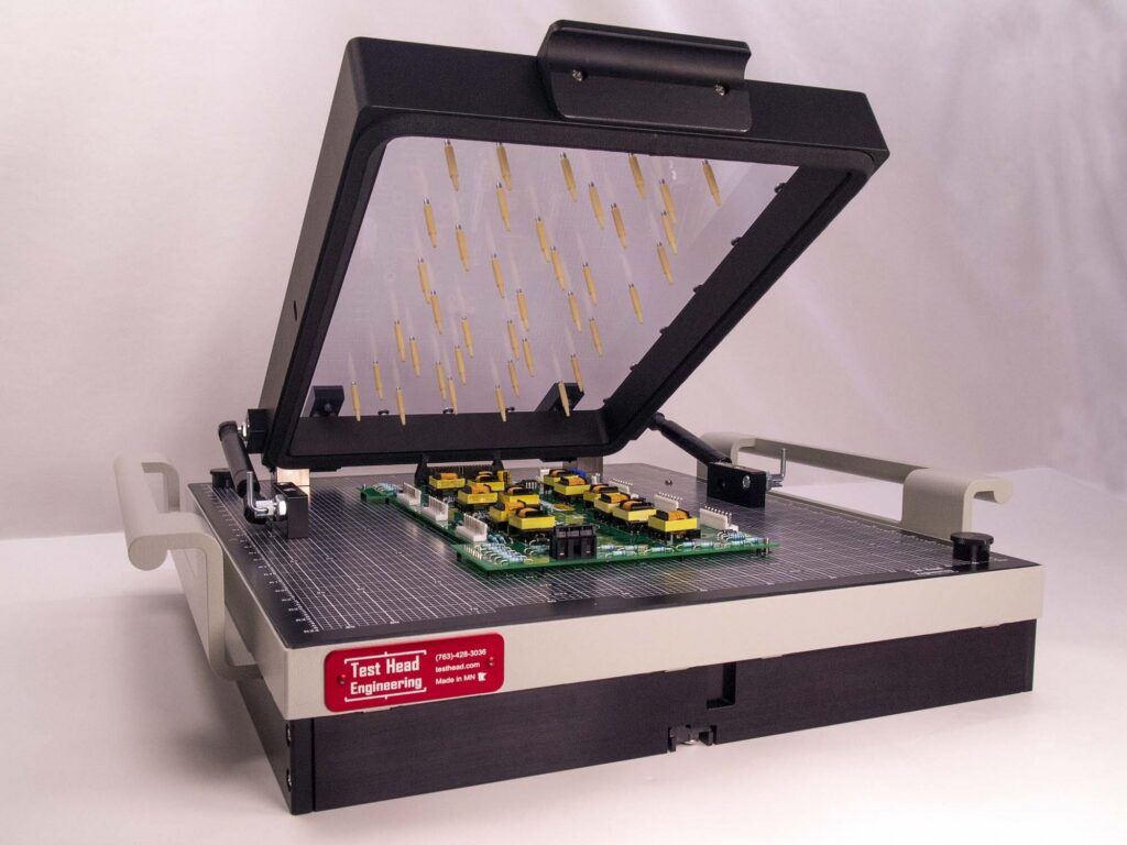
Instead of powering up the entire board to see if the overall system boots (which is known as Functional Testing or FCT), ICT uses a customized bed of spring-loaded pogo pins to press against dedicated test points on the PCB. It isolates and measures every component—resistors, capacitors, inductors, diodes, and integrated circuits—one by one.
The key word here is In-Circuit. Through a technique called guarding, the ICT system electronically insulates neighboring components so it can measure a single 100nF capacitor embedded deep within a complex schematic without interference from parallel circuit paths.
How an ICT System Works: The "Bed of Nails"
Here is the physical sequence of how a PCB undergoes an In-Circuit Test on the production line:
The assembled PCB is placed onto the custom ICT fixture (often called the “bed of nails”). The fixture contains hundreds or thousands of spring-loaded metal pogo pins positioned to match the exact X/Y coordinates of the test pads designed on the bottom layer of the board.
A vacuum suction lid or pneumatic top plate presses down on the PCB. This forces every test point pad firmly against its corresponding spring-loaded pogo pin, establishing a clean, low-resistance electrical contact.
The ICT system executes a pre-programmed test script in seconds. Matrix switches rapidly route signals through the pins to measure passive values (resistance, capacitance, inductance), verify diode junctions, test for short circuits, and check power rail voltages.
If a net fails—for instance, if pin 42 shows an open circuit—the software instantly flags the exact component location (e.g., “R15 value out of tolerance: Expected 1kΩ, Measured 0Ω – Short”). The board is routed directly to a rework technician for quick repair.
What Defects Does an ICT Catch?
Component-Level Faults:
Incorrect Component Values: A 1kΩ resistor placed where a 10kΩ resistor belonged.
Out-of-Tolerance Components: Passive components that drifted beyond their specified percentage tolerance.
Damaged / Dead Components: ICs or diodes that were killed by ESD (Electrostatic Discharge) or thermal stress during reflow.
- Reversed Polarity: Diodes, tantalum capacitors, or ICs installed backwards that still pass optical checks.
Process & Assembly Faults:
Solder Bridges / Shorts: Accidental solder connections shorting two adjacent traces or power to ground.
Open Circuits (Cold Joints): Unsoldered leads or cracked solder joints that fail to make electrical contact.
Missing Components: SMT components that blew off or were skipped by the pick-and-place machine.
Traditional ICT vs. Flying Probe Testing
Building a custom “bed of nails” fixture requires CNC machining and manual wiring, which can cost anywhere from $3,000 to $20,000+ per fixture. For small production runs or prototypes, this upfront NRE (Non-Recurring Engineering) cost isn’t practical.
That is where Flying Probe Testing comes in as an alternative.
| Feature | Traditional ICT (Bed of Nails) | Flying Probe Testing |
|---|---|---|
| Mechanics | Fixed bed of hundreds/thousands of stationary pogo pins. | 4 to 8 robotic probes that fly around the board at high speed. |
| Test Speed | Ultra-Fast: Tests a complex board in 10–30 seconds. | Slower: Takes 5–15+ minutes per board. |
| Fixture Cost | High upfront cost ($3,000–$20,000+). | $0 Fixture Cost: Purely software-driven via CAD data. |
| Best For | High-volume, mass production (thousands of units). | Low-volume prototypes, quick-turn R&D, frequent design changes. |
Pros and Cons of In-Circuit Testing
Advantages:
Unmatched Speed: Takes less than a minute to thoroughly test a board with thousands of components.
Precise Diagnostics: Doesn’t just say “the board doesn’t turn on”—it tells the repair technician exactly which resistor or pin failed.
High Defect Coverage: Catches up to 95%+ of assembly and component-level manufacturing defects.
Firmware Programming: Modern ICT fixtures can also flash basic bootloaders or microcode onto onboard flash memory during the test cycle.
Disadvantages:
High Initial Cost: Expensive fixtures and dedicated test machines (like Teradyne or Keysight platforms).
Design Constraints (DFTa / DFM): Designers must explicitly add physical test pads (typically 0.7mm to 1.0mm in diameter) to almost every net, which uses up precious PCB layout space.
Design Inflexibility: If you change the PCB layout or move a component in a revision, you may have to scrap the old fixture and pay for a new one.
Summary
An In-Circuit Test (ICT) is the ultimate quality firewall for high-volume electronics manufacturing. By using a bed-of-nails fixture to contact individual test pads, ICT isolates every component and net to catch assembly errors before boards undergo final functional testing.
If you are scaling up to mass production (typically 5,000+ units per run), investing in an ICT fixture will pay for itself rapidly by preventing costly field returns and streamlining factory floor repairs.
FAQ
Can ICT replace Functional Testing (FCT)?
No. ICT verifies that the components are correct and soldered down properly, but it does not run the board under full operating conditions (e.g., executing high-speed communication protocols or running full system firmware). High-reliability industries (like automotive or medical) use ICT and FCT sequentially.
What is a “Test Pad” in ICT layout design?
A test pad is a small, dedicated exposed copper circle on the PCB specifically designed for a pogo pin to strike. Guidelines generally recommend a minimum diameter of 0.7mm to 1.0mm, spaced at least 1.27mm apart, to ensure reliable physical contact without damaging adjacent traces.
What happens if a board design changes slightly after building an ICT fixture?
If the board revision only changes component values (e.g., swapping a 10k resistor for a 4.7k resistor), you only need to update the ICT software script. However, if component positions or trace routes move—changing the X/Y location of test pads—the physical fixture must be re-drilled or completely remade.

